
EP1S20F672I7N
| Part Description |
Stratix® Field Programmable Gate Array (FPGA) IC 426 1669248 18460 672-BBGA |
|---|---|
| Quantity | 106 Available (as of October 8, 2026) |

| Product Category | Field Programmable Gate Array (FPGA) |
|---|---|
| Manufacturer | Intel |
| Manufacturing Status | Obsolete |
| Manufacturer Standard Lead Time | Contact Us |
| Datasheet |
Specifications & Environmental
| Device Package | 672-FBGA (27x27) | Grade | Industrial | Operating Temperature | -40°C – 100°C | ||
|---|---|---|---|---|---|---|---|
| Package / Case | 672-BBGA | Number of I/O | 426 | Voltage | 1.425 V - 1.575 V | ||
| Mounting Method | Surface Mount | RoHS Compliance | Unknown | REACH Compliance | REACH Unaffected | ||
| Moisture Sensitivity Level | 3 (168 Hours) | Number of LABs/CLBs | 1846 | Number of Logic Elements/Cells | 18460 | ||
| Number of Gates | N/A | ECCN | 3A991D | HTS Code | 8542.39.0001 | ||
| Qualification | N/A | Total RAM Bits | 1669248 |
Overview of EP1S20F672I7N – Stratix Field Programmable Gate Array (FPGA), 672-BBGA
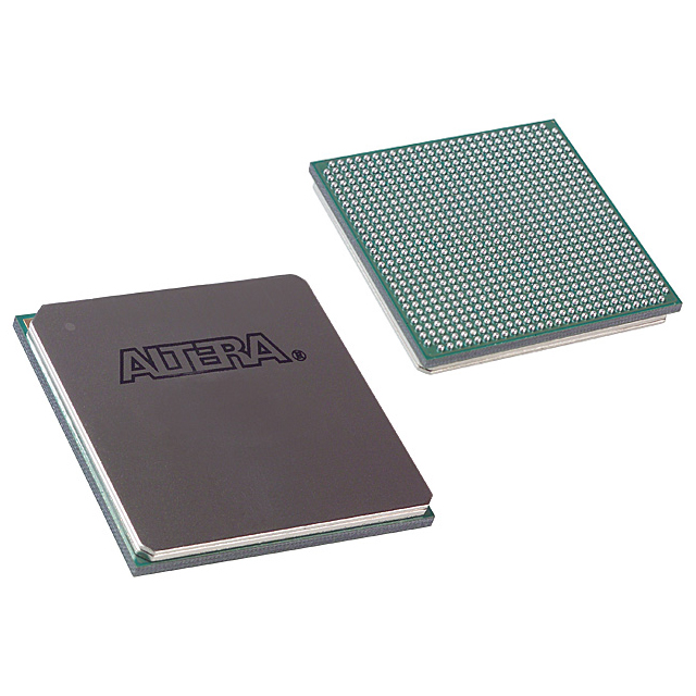
The EP1S20F672I7N is a Stratix® FPGA in a 672-ball BGA package designed for industrial applications requiring reconfigurable logic and substantial on-chip resources. Its architecture delivers a balance of logic density, embedded memory, and I/O capacity suitable for demanding system designs that must operate across a wide temperature range.
With 18,460 logic elements, approximately 1.67 Mbits of embedded memory, and 426 I/Os, this device targets designs that need high integration, flexible I/O, and on-chip memory for buffering, protocol handling, and custom processing.
Key Features
- Core Logic 18,460 logic elements provide programmable capacity for implementing complex digital logic and state machines.
- Embedded Memory Approximately 1.67 Mbits of on-chip RAM to support frame buffering, FIFOs, and local data storage without external memory for many use cases.
- I/O Capacity 426 I/O pins offer extensive connectivity for parallel buses, control signals, and interface routing in high-density systems.
- Package & Mounting 672-ball BGA (supplier device package: 672-FBGA, 27×27) in a surface-mount form factor for compact board implementation.
- Power Core voltage range of 1.425 V to 1.575 V to match system power domains and regulator choices.
- Industrial Temperature Range Rated for −40 °C to 100 °C operation, suitable for industrial environments and extended-temperature applications.
- Standards & Tools Support Datasheet documents IEEE Std. 1149.1 (JTAG) boundary-scan support and on-chip logic analysis capability (SignalTap II), aiding board bring-up and debug.
- High-Speed I/O & Clocking Device documentation includes support for high-speed differential I/O, PLLs and clock networks, and external RAM interfacing for synchronous system integration.
- Environmental Compliance RoHS compliant.
Typical Applications
- Industrial Control Use in motor control, PLC interfaces, and process-control logic where extended temperature operation and high I/O counts are required.
- Data Buffering & Protocol Bridging On-chip RAM and abundant I/Os enable packet buffering, protocol conversion, and custom interface bridging without immediate dependence on external memory.
- High-Speed I/O Systems Suitable for designs that require differential I/O and programmable clocking resources for timing-critical signal paths and interfaces.
Unique Advantages
- Substantial Logic Density: 18,460 logic elements allow implementation of complex control, processing, and glue-logic functions in a single device, reducing board-level component count.
- Integrated On-Chip Memory: Approximately 1.67 Mbits of embedded RAM reduces reliance on external RAM for many buffering and temporary storage needs, simplifying BOM and layout.
- Extensive I/O Count: 426 I/Os provide flexibility to interface multiple peripherals and buses directly, enabling highly integrated system designs.
- Industrial Reliability: Specified for −40 °C to 100 °C operation and supplied in a robust BGA package for reliable operation in industrial environments.
- Debug & Configuration Support: JTAG boundary-scan and on-chip logic analysis (SignalTap II) support facilitate faster bring-up, in-system debug, and iterative development.
- RoHS Compliant: Environmental compliance supports broader regulatory acceptance and manufacturing requirements.
Why Choose EP1S20F672I7N?
The EP1S20F672I7N positions itself as a high-capacity, industrial-grade Stratix FPGA that combines significant logic resources, embedded memory, and a large I/O footprint in a compact 672-BBGA package. Its documented support for JTAG boundary-scan, on-chip logic analysis, high-speed I/O, and comprehensive clocking resources makes it suitable for teams developing complex, timing-sensitive designs that demand on-board programmability and robust debug capabilities.
This device is a practical option for engineering teams and procurement seeking a reconfigurable, RoHS-compliant FPGA that supports extended temperature operation and high integration to simplify system architecture and reduce external components.
Request a quote or submit an inquiry to get pricing and availability information for EP1S20F672I7N.

























Date Founded: 1968
Headquarters: Santa Clara, California, USA
Employees: 130,000+
Revenue: $54.23 Billion
Certifications and Memberships: ISO9001:2015, ISO14001:2015, ISO17025:2017, ISO27001:2022, ISO45001:2018, ISO50001:2018


