
EP1SGX25DF672C7N
| Part Description |
Stratix® GX Field Programmable Gate Array (FPGA) IC 455 1944576 25660 672-BBGA |
|---|---|
| Quantity | 606 Available (as of June 15, 2026) |
| Product Category | Field Programmable Gate Array (FPGA) |
|---|---|
| Manufacturer | Intel |
| Manufacturing Status | Obsolete |
| Manufacturer Standard Lead Time | Contact Us |
| Datasheet |
Specifications & Environmental
| Device Package | 672-FBGA (27x27) | Grade | Commercial | Operating Temperature | 0°C – 85°C | ||
|---|---|---|---|---|---|---|---|
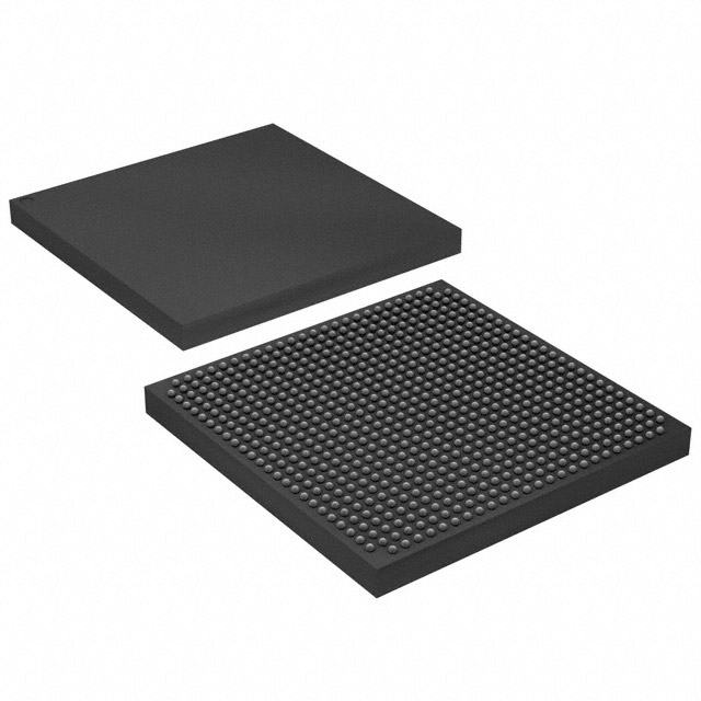
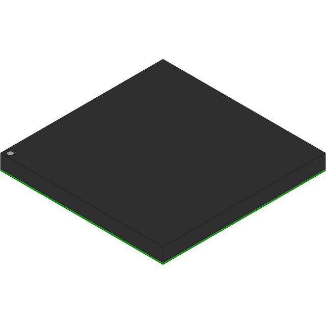
| Package / Case | 672-BBGA | Number of I/O | 455 | Voltage | 1.425 V - 1.575 V | ||
| Mounting Method | Surface Mount | RoHS Compliance | Unknown | REACH Compliance | REACH Unknown | ||
| Moisture Sensitivity Level | 3 (168 Hours) | Number of LABs/CLBs | 2566 | Number of Logic Elements/Cells | 25660 | ||
| Number of Gates | N/A | ECCN | 3A001A7A | HTS Code | 8542.39.0001 | ||
| Qualification | N/A | Total RAM Bits | 1944576 |
Overview of EP1SGX25DF672C7N – Stratix® GX FPGA, 25,660 logic elements, 455 I/O, 672-BBGA
The EP1SGX25DF672C7N is a Stratix® GX family field-programmable gate array (FPGA) from Intel, optimized for high-performance, programmable logic and high-speed serial I/O. It delivers 25,660 logic elements and approximately 1.94 Mbits of on-chip RAM in a 672-ball BGA package, making it suitable for demanding communications, backplane and protocol-bridging designs.
Designed on the Stratix GX architecture, this device combines a high-density logic array with the family’s transceiver and SERDES capabilities and a 1.5-V logic technology operating from a 1.425 V to 1.575 V supply, enabling integration of complex, timing-critical functions within a single FPGA.
Key Features
- Logic Capacity 25,660 logic elements for implementing mid-to-high complexity digital logic and state machines.
- Embedded Memory Approximately 1.94 Mbits of on-chip RAM to support packet buffering, FIFOs and on-chip data storage.
- High-speed Transceivers (family capability) Stratix GX family transceivers support 500 Mbps to 3.1875 Gbps full-duplex operation with clock data recovery (CDR) and embedded SERDES for protocol bridging and serial links.
- I/O Density 455 I/O pins to interface with external memory, peripherals, and multi-lane serial PHYs.
- Clocking and DSP Resources (family capability) Dedicated DSP and PLL resources in the Stratix GX family provide hardware acceleration for multiply-accumulate and high-speed clock management tasks.
- Package and Mounting 672-BBGA package (supplier device package listed as 672-FBGA (27x27)); surface-mount device for compact board-level integration.
- Power and Supply Core supply range 1.425 V to 1.575 V to match high-performance 1.5-V logic requirements.
- Operating Range and Compliance Commercial temperature grade (0 °C to 85 °C) and RoHS compliant.
Typical Applications
- High-speed backplane interfaces Use the device’s high-density logic and Stratix GX transceiver capabilities (family-level) to implement switched fabric and backplane protocol endpoints.
- Chip-to-chip bridging Implement protocol translation and SERDES-based links between ASICs, processors and other FPGAs using on-chip logic and embedded memory.
- Communications protocol bridging Support protocol adaptation and packet processing for interfaces such as Ethernet and Fibre Channel as part of network equipment designs (supported at the family level).
- High-performance data buffering and processing Leverage approximately 1.94 Mbits of embedded RAM and abundant logic elements for packet buffering, LUT-based preprocessing and custom data paths.
Unique Advantages
- Balanced logic and memory 25,660 logic elements paired with ~1.94 Mbits of on-chip RAM enable complex control and data-path implementations without immediate reliance on external memory.
- High I/O count 455 I/O pins give flexibility to connect wide parallel buses, multiple interfaces, or numerous serial lanes without extensive board-level multiplexing.
- Family-level serial capability Stratix GX transceiver technology (500 Mbps–3.1875 Gbps) supports high-speed serial links and protocol-aware features such as 8B/10B encoding and channel bonding.
- Compact, production-ready packaging 672-ball BGA in a surface-mount form factor (supplier: 672-FBGA (27x27)) simplifies PCB routing density for space-constrained systems.
- RoHS compliant Environmentally compliant material status suitable for standard commercial production flows.
Why Choose EP1SGX25DF672C7N?
The EP1SGX25DF672C7N positions itself as a mid-to-high density Stratix GX FPGA option that combines substantial logic capacity and embedded RAM with a high I/O count and family-level high-speed transceiver features. It is well-suited for designers building communications equipment, backplane interfaces, protocol bridges, and other systems that require integrated serial and parallel processing in a single, RoHS-compliant device.
With commercial temperature rating, a 672-ball BGA package for dense board layouts, and a defined core supply range, this FPGA offers predictable integration characteristics and long-term design scalability within the Stratix GX family architecture.
Request a quote or submit a parts inquiry to receive pricing, availability, and technical support for EP1SGX25DF672C7N.


Date Founded: 1968
Headquarters: Santa Clara, California, USA
Employees: 130,000+
Revenue: $54.23 Billion
Certifications and Memberships: ISO9001:2015, ISO14001:2015, ISO17025:2017, ISO27001:2022, ISO45001:2018, ISO50001:2018


