
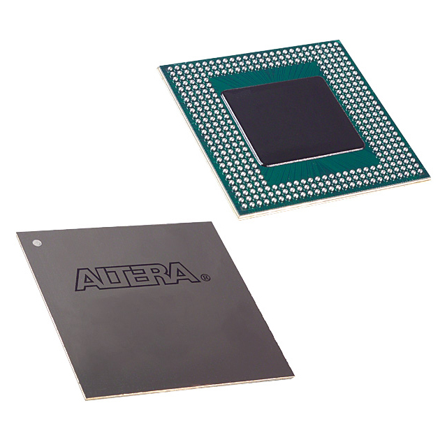
EP20K200EBC356-3
| Part Description |
APEX-20KE® Field Programmable Gate Array (FPGA) IC 271 106496 8320 356-LBGA |
|---|---|
| Quantity | 1,801 Available (as of June 15, 2026) |

| Product Category | Field Programmable Gate Array (FPGA) |
|---|---|
| Manufacturer | Intel |
| Manufacturing Status | Obsolete |
| Manufacturer Standard Lead Time | Contact Us |
| Datasheet |
Specifications & Environmental
| Device Package | 356-BGA (35x35) | Grade | Commercial | Operating Temperature | 0°C – 85°C | ||
|---|---|---|---|---|---|---|---|
| Package / Case | 356-LBGA | Number of I/O | 271 | Voltage | 1.71 V - 1.89 V | ||
| Mounting Method | Surface Mount | RoHS Compliance | Unknown | REACH Compliance | REACH Unaffected | ||
| Moisture Sensitivity Level | 3 (168 Hours) | Number of LABs/CLBs | 832 | Number of Logic Elements/Cells | 8320 | ||
| Number of Gates | 526000 | ECCN | 3A001A2A | HTS Code | 8542.39.0001 | ||
| Qualification | N/A | Total RAM Bits | 106496 |
Overview of EP20K200EBC356-3 – APEX-20KE® Field Programmable Gate Array (FPGA) IC 271 106496 8320 356-LBGA
The EP20K200EBC356-3 is an APEX-20KE family FPGA offering a MultiCore architecture that integrates look-up table (LUT) logic and embedded system blocks (ESBs) for memory and product-term functions. It targets designs that require significant on-chip logic and embedded memory alongside flexible I/O and clock management.
With 8,320 logic elements, approximately 106,496 bits of embedded memory, and 271 user I/O pins in a 356-LBGA package, this device is suitable for applications needing compact, programmable logic with multi-voltage I/O support and configurable clock resources.
Key Features
- Core architecture MultiCore architecture combining LUT logic and ESB resources for register‑intensive and memory‑centric functions.
- Logic capacity 8,320 logic elements and 526,000 system gates provide significant combinational and sequential logic density for mid-range designs.
- Embedded memory Approximately 106,496 bits of on-chip RAM available for FIFOs, dual-port RAM, and content-addressable memory (CAM) implementations via ESBs.
- I/O and interface flexibility 271 user I/O pins with MultiVolt I/O interface support for interoperability with 1.8 V, 2.5 V, 3.3 V, and 5.0 V devices (family-level support documented in the datasheet).
- Clock management Flexible clock resources including up to four phase-locked loops (PLLs), a built-in low-skew clock tree and up to eight global clock signals for complex timing domains.
- Power and supply Internal supply centered around 1.8 V with specified device supply range of 1.71 V to 1.89 V and device-level low-power features described in the family documentation.
- Package and mounting 356‑ball LFBGA (35 mm × 35 mm) surface-mount package suitable for high‑density board layouts.
- Commercial temperature range Rated for 0 °C to 85 °C operation for commercial applications.
- Compliance RoHS compliant.
Typical Applications
- Memory interface and buffering Implement FIFOs, dual-port RAM, and memory controllers using the device’s embedded system blocks and on-chip RAM.
- Custom I/O bridging and protocol handling MultiVolt I/O support and abundant I/O pins enable protocol conversion and interface bridging across different logic levels.
- Embedded logic and control LUT-based logic and dedicated carry chains make the device suitable for custom control logic, state machines, and peripheral offload.
- Mid-range system integration System-on-programmable-chip (SOPC) style integration combining logic and embedded memory for compact system designs.
Unique Advantages
- Integrated memory and logic: Embedded system blocks provide on-chip RAM and product-term logic, reducing the need for external memory in many designs.
- Significant on-chip resources: 8,320 logic elements and roughly 106 kbits of embedded memory support moderate-density logic and data buffering within a single device.
- Flexible clocking: Multiple PLLs and a low-skew clock tree enable reliable multi-domain timing strategies without external clock management ICs.
- Multi-voltage I/O compatibility: Support for multiple I/O voltage levels enables direct interfacing to a broad range of peripheral devices.
- Compact BGA package: 356-BGA (35 × 35 mm) package allows high I/O count and denser PCB routing in space-constrained designs.
- Commercial-grade suitability: Rated for 0 °C to 85 °C operation and RoHS compliant for mainstream electronic products.
Why Choose EP20K200EBC356-3?
The EP20K200EBC356-3 provides a balanced combination of logic density, embedded memory, and flexible I/O in the APEX‑20K family architecture. It is well suited for designers who need a mid-range FPGA that integrates LUT-based logic, ESB memory functions, and robust clocking features within a compact 356-LBGA package.
For projects requiring embedded FIFOs, custom protocol handling, or consolidated system logic with multi-voltage I/O compatibility, this device offers measurable on-chip resources and family-documented features that simplify board-level design and reduce external component count.
Request a quote or submit an RFQ to begin procurement and evaluate EP20K200EBC356-3 for your next design.


Date Founded: 1968
Headquarters: Santa Clara, California, USA
Employees: 130,000+
Revenue: $54.23 Billion
Certifications and Memberships: ISO9001:2015, ISO14001:2015, ISO17025:2017, ISO27001:2022, ISO45001:2018, ISO50001:2018


