
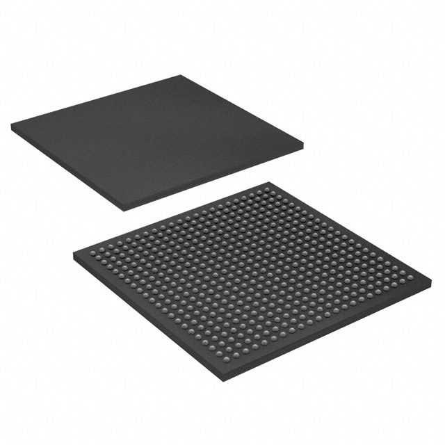
EP20K200EFC484-1
| Part Description |
APEX-20KE® Field Programmable Gate Array (FPGA) IC 376 106496 8320 484-BBGA |
|---|---|
| Quantity | 341 Available (as of June 16, 2026) |

| Product Category | Field Programmable Gate Array (FPGA) |
|---|---|
| Manufacturer | Intel |
| Manufacturing Status | Obsolete |
| Manufacturer Standard Lead Time | Contact Us |
| Datasheet |
Specifications & Environmental
| Device Package | 484-FBGA (23x23) | Grade | Commercial | Operating Temperature | 0°C – 85°C | ||
|---|---|---|---|---|---|---|---|
| Package / Case | 484-BBGA | Number of I/O | 376 | Voltage | 1.71 V - 1.89 V | ||
| Mounting Method | Surface Mount | RoHS Compliance | RoHS non-compliant | REACH Compliance | REACH Unaffected | ||
| Moisture Sensitivity Level | 3 (168 Hours) | Number of LABs/CLBs | 832 | Number of Logic Elements/Cells | 8320 | ||
| Number of Gates | 526000 | ECCN | 3A991D | HTS Code | 8542.39.0001 | ||
| Qualification | N/A | Total RAM Bits | 106496 |
Overview of EP20K200EFC484-1 – APEX-20KE® Field Programmable Gate Array (FPGA) IC 376 106496 8320 484-BBGA
The EP20K200EFC484-1 is an APEX-20KE family FPGA from Intel, delivering a MultiCore architecture that integrates lookup-table (LUT) logic, product-term logic, and embedded memory blocks for system-on-a-programmable-chip designs. This device targets applications that require a balance of logic capacity, embedded RAM and a high I/O count within a compact 484-BBGA package.
With 8,320 logic elements, approximately 0.106 Mbits of embedded memory, and 376 user I/O pins, the EP20K200EFC484-1 is suited for mid-density programmable logic tasks where flexible I/O standards, clock management and power efficiency matter.
Key Features
- Core architecture — MultiCore architecture integrating LUT logic, product-term logic and embedded system blocks (ESBs) for register-intensive and combinatorial functions.
- Logic capacity — 8,320 logic elements and a maximum system gate equivalent of 526,000 provide mid-range programmable logic resources.
- Embedded memory — 106,496 bits of on-chip RAM (approximately 0.106 Mbits) available for FIFOs, dual-port RAM or CAM implementations using ESBs.
- I/O and packaging — 376 user I/O pins in a 484-BBGA package (supplier package 484-FBGA, 23×23) with surface-mount mounting suitable for compact board designs.
- MultiVolt I/O support — I/O interface support for 1.8 V, 2.5 V, 3.3 V and 5.0 V signaling to interface with a wide range of peripherals and memories.
- Clock management — Up to four PLLs, a built-in low-skew clock tree, up to eight global clock signals, and features such as ClockLock, ClockBoost and ClockShift for flexible phase, multiplication and delay control.
- High-speed interface support — I/O features and signaling support documented for high-speed external memories and bus applications, including PCI 3.3-V operation at 33 or 66 MHz (per device family documentation).
- Power and temperature — Designed for low-power operation with an internal supply range of 1.71 V to 1.89 V and a commercial-grade operating temperature range of 0 °C to 85 °C.
- Regulatory — RoHS compliant, supporting environmentally regulated manufacturing requirements.
Typical Applications
- Data buffering and memory bridging — Embedded RAM and ESBs can implement FIFOs and dual-port RAM for interfacing between different clock domains and memory types.
- High-speed I/O and bus control — MultiVolt I/O and documented PCI 3.3-V operation enable use in bus-bridging, peripheral control and interface conversion tasks.
- Signal processing and control logic — LUT-based logic and dedicated carry chains support register-intensive functions and arithmetic building blocks for communication and embedded control subsystems.
- Custom embedded systems — The combination of logic elements, embedded memory and PLL-based clock management suits mid-density system-on-chip implementations and prototyping.
Unique Advantages
- Balanced mid-range capacity: 8,320 logic elements and ~0.106 Mbits of embedded memory provide a practical resource set for midsize designs without excessive board-level complexity.
- Flexible I/O connectivity: Support for multiple voltage domains (1.8 V–5.0 V) simplifies integration with legacy and modern peripherals, reducing interface translator requirements.
- Advanced clocking: Up to four PLLs and multiple clock features (ClockLock, ClockBoost, ClockShift) enable precise timing control for multi-domain systems.
- Compact, surface-mount package: The 484-BBGA (484-FBGA 23×23) package offers high I/O density in a footprint suitable for space-constrained PCBs.
- Power-aware design: Low-power operation modes and a narrow internal supply range (1.71 V–1.89 V) support energy-conscious system designs.
- Standards-oriented I/O: I/O feature set and family documentation include compliance notes for high-speed memory interfaces and PCI signaling, helping streamline system connectivity.
Why Choose EP20K200EFC484-1?
The EP20K200EFC484-1 positions itself as a mid-density FPGA option within the APEX-20KE family, combining 8,320 logic elements, approximately 0.106 Mbits of embedded RAM, and 376 user I/Os in a 484-BBGA form factor. Its MultiCore architecture and ESB capabilities let designers implement a mix of register-intensive logic and embedded memory functions on a single device.
This device is well suited for engineers building compact, power-aware embedded systems, interface bridges, and mid-range communication or control designs that require flexible clocking and multi-voltage I/O support. RoHS compliance and commercial-grade temperature ratings align it with typical production and procurement requirements.
Request a quote or submit a purchase inquiry to receive pricing, availability and lead-time information for the EP20K200EFC484-1. Our team can provide part-specific support and ordering guidance to help move your design forward.


Date Founded: 1968
Headquarters: Santa Clara, California, USA
Employees: 130,000+
Revenue: $54.23 Billion
Certifications and Memberships: ISO9001:2015, ISO14001:2015, ISO17025:2017, ISO27001:2022, ISO45001:2018, ISO50001:2018


