
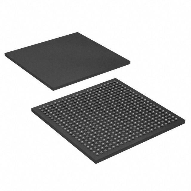
EP20K200EFC484-1X
| Part Description |
APEX-20KE® Field Programmable Gate Array (FPGA) IC 376 106496 8320 484-BBGA |
|---|---|
| Quantity | 1,388 Available (as of June 15, 2026) |

| Product Category | Field Programmable Gate Array (FPGA) |
|---|---|
| Manufacturer | Intel |
| Manufacturing Status | Obsolete |
| Manufacturer Standard Lead Time | Contact Us |
| Datasheet |
Specifications & Environmental
| Device Package | 484-FBGA (23x23) | Grade | Commercial | Operating Temperature | 0°C – 85°C | ||
|---|---|---|---|---|---|---|---|
| Package / Case | 484-BBGA | Number of I/O | 376 | Voltage | 1.71 V - 1.89 V | ||
| Mounting Method | Surface Mount | RoHS Compliance | RoHS non-compliant | REACH Compliance | REACH Unaffected | ||
| Moisture Sensitivity Level | 3 (168 Hours) | Number of LABs/CLBs | 832 | Number of Logic Elements/Cells | 8320 | ||
| Number of Gates | 526000 | ECCN | 3A991D | HTS Code | 8542.39.0001 | ||
| Qualification | N/A | Total RAM Bits | 106496 |
Overview of EP20K200EFC484-1X – APEX-20KE® FPGA, 484-BBGA, 376 I/O
The EP20K200EFC484-1X is an APEX-20KE family Field Programmable Gate Array (FPGA) provided in a 484-BBGA package. It uses a MultiCore architecture that integrates look-up table (LUT) logic, product-term logic, and embedded system blocks (ESBs) to support register‑intensive and memory‑centric functions.
With 8,320 logic elements, approximately 0.106 Mbits of embedded memory (106,496 bits), 376 user I/O pins, and support for advanced clock management, this device targets designs that require moderate gate density, embedded RAM, and flexible I/O and clocking resources within commercial-temperature environments.
Key Features
- Core Architecture MultiCore architecture combining LUT logic, product-term logic and embedded system blocks for mixed register and memory functions.
- Logic Capacity Approximately 8,320 logic elements and 526,000 system gates provide the programmable logic resources for medium-density FPGA designs.
- Embedded Memory Approximately 106,496 bits of on-chip RAM suitable for FIFOs, dual-port RAMs and other memory functions implemented in ESBs.
- I/O and Interfaces 376 user I/O pins with MultiVolt I/O support and programmable I/O features to interface with a range of external devices and memory types.
- Clock Management Flexible clock circuitry including up to four PLLs, support for multiple global clocks and programmable clock phase/delay features to manage timing and clock distribution.
- Power Low‑power design focus with an internal supply range centered at 1.8 V and VCCIO support aligned to MultiVolt interfaces; device supply specified at 1.71 V to 1.89 V.
- Package and Mounting Surface-mount 484-BBGA package (supplier device package 484-FBGA, 23×23) for board-level integration.
- Operating Range and Compliance Commercial grade operation from 0 °C to 85 °C and RoHS compliant.
Typical Applications
- Memory Interface and Buffering Implement FIFO buffers, dual-port RAM and memory controllers using embedded system blocks and on-chip RAM.
- Bus and Peripheral Bridging Use programmable I/O and MultiVolt support to bridge or interface between different bus standards and peripheral devices.
- Clocked Logic and Timing Control Leverage multiple PLLs and global clock resources for designs requiring flexible clocking, phase shifting and low-skew distribution.
- Custom Logic for Embedded Systems Deploy the device’s LUT logic and product-term capabilities for control, signal processing, and glue logic in commercial embedded products.
Unique Advantages
- Integrated Memory and Logic: Combines embedded RAM (≈106,496 bits) with 8,320 logic elements to implement memory‑heavy functions without external components.
- Flexible Clocking: Up to four PLLs and multiple global clocks simplify timing architectures and enable programmable clock phase and delay control.
- MultiVolt I/O Support: Programmable I/O levels and clamp/slew control enable interfacing with a variety of external voltage domains.
- Commercial-Grade Temperature: Rated for 0 °C to 85 °C operation, suitable for mainstream commercial applications.
- Board-Level Integration: Surface-mount 484-BBGA package (484-FBGA, 23×23) balances pin count (376 I/O) with compact footprint for populated PCBs.
- Standards and I/O Features: Design includes features for high-speed I/O and support for advanced signalling and memory interfaces described in the APEX-20K family documentation.
Why Choose EP20K200EFC484-1X?
The EP20K200EFC484-1X positions itself as a medium-density, commercially rated FPGA that brings together logic richness, embedded memory and flexible I/O/clock resources in a compact 484-BBGA package. It is tailored for engineers who need integrated memory blocks, multiple clocking options and significant I/O in a commercially available device.
This part is well suited for designs that require programmable logic and embedded RAM for buffering, protocol bridging, and custom logic functions where commercial temperature range and RoHS compliance are appropriate procurement criteria.
If you would like pricing, availability, or a formal quote for EP20K200EFC484-1X, request a quote or submit an RFQ and our team will respond with details.


Date Founded: 1968
Headquarters: Santa Clara, California, USA
Employees: 130,000+
Revenue: $54.23 Billion
Certifications and Memberships: ISO9001:2015, ISO14001:2015, ISO17025:2017, ISO27001:2022, ISO45001:2018, ISO50001:2018


