
EP20K200EFC484-1N
| Part Description |
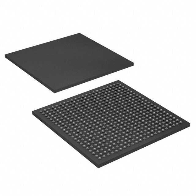
APEX-20KE® Field Programmable Gate Array (FPGA) IC 376 106496 8320 484-BBGA |
|---|---|
| Quantity | 1,046 Available (as of June 18, 2026) |

| Product Category | Field Programmable Gate Array (FPGA) |
|---|---|
| Manufacturer | Intel |
| Manufacturing Status | Obsolete |
| Manufacturer Standard Lead Time | Contact Us |
| Datasheet |
Specifications & Environmental
| Device Package | 484-FBGA (23x23) | Grade | Commercial | Operating Temperature | 0°C – 85°C | ||
|---|---|---|---|---|---|---|---|
| Package / Case | 484-BBGA | Number of I/O | 376 | Voltage | 1.71 V - 1.89 V | ||
| Mounting Method | Surface Mount | RoHS Compliance | Unknown | REACH Compliance | REACH Unaffected | ||
| Moisture Sensitivity Level | 3 (168 Hours) | Number of LABs/CLBs | 832 | Number of Logic Elements/Cells | 8320 | ||
| Number of Gates | 526000 | ECCN | 3A001A2A | HTS Code | 8542.39.0001 | ||
| Qualification | N/A | Total RAM Bits | 106496 |
Overview of EP20K200EFC484-1N – APEX-20KE® Field Programmable Gate Array (FPGA) IC, 484-BBGA
The EP20K200EFC484-1N is an APEX-20KE family FPGA from Intel designed for system-level integration of logic and embedded memory. Built on a MultiCore architecture that combines look-up table (LUT) logic, product-term logic and embedded system blocks, this device targets applications requiring configurable logic, embedded RAM and flexible I/O.
With 8,320 logic elements, 106,496 bits of on-chip RAM and 376 user I/O pins in a 484-BBGA package, the device supports designs that need moderate logic density, dedicated memory resources and interoperable I/O voltage levels while operating within a commercial temperature range.
Key Features
- Core architecture MultiCore architecture integrating LUT logic, product-term logic and embedded memory for a mix of register- and combinatorial-intensive functions.
- Logic resources 8,320 logic elements and up to 526,000 maximum system gates provide scalable fabric capacity for mid-density FPGA designs.
- Embedded memory Total on-chip RAM of 106,496 bits suitable for FIFOs, dual-port RAM and other memory-centric functions.
- I/O and interfacing 376 user I/O pins with MultiVolt I/O support (family-level support for 1.8 V, 2.5 V, 3.3 V and 5.0 V) and features for high-speed external memory and bus interfaces.
- Clock management Flexible clock circuitry including up to four PLLs, low-skew clock tree and support for multiple global clock signals.
- Power and supply Internal/core supply around 1.8 V (product supply range 1.71 V to 1.89 V) with on-device power-saving options for embedded system blocks.
- Package and mounting 484-BBGA (supplier package 484-FBGA, 23 × 23) surface-mount package for dense board integration.
- Operating grade Commercial grade device rated for 0 °C to 85 °C operation and compliant with RoHS requirements.
Typical Applications
- Memory interface controllers Implement DDR SDRAM or ZBT SRAM interfaces using the device’s embedded memory and high-speed I/O capabilities.
- PCI and bus bridge logic Use the device’s I/O feature set and configurable logic to implement PCI-compliant bus interfaces and protocol bridging.
- Signal processing and data aggregation Deploy the FPGA’s LUT-based logic, dedicated memory blocks and clock management for buffering, aggregation and preprocessing of data streams.
- High-speed serial and differential I/O Leverage LVDS-capable I/O and high-speed signaling support for channelized data links and board-level transceiver functions.
Unique Advantages
- Integrated memory and logic: 106,496 bits of embedded RAM combined with 8,320 logic elements reduce the need for external memory in many buffering and control functions.
- Flexible I/O voltage support: MultiVolt I/O capability enables interfacing to a broad range of system voltages without external level translators in many cases.
- Comprehensive clock controls: Multiple PLLs and a low-skew clock tree simplify clock distribution and timing management for synchronous designs.
- Compact BGA package: 484-BBGA surface-mount package delivers a high pin count and compact footprint for space-constrained boards.
- Commercial-grade reliability: Rated for 0 °C to 85 °C operation and RoHS compliant for standard commercial deployments.
Why Choose EP20K200EFC484-1N?
The EP20K200EFC484-1N offers a balanced combination of mid-range logic density, built-in RAM and flexible I/O in a compact BGA package. Its MultiCore architecture and clock management features make it well suited for designs that require integrated memory handling, protocol bridging and deterministic clocking across multiple domains.
This device is suited to engineers developing commercial embedded systems who need a configurable, RoHS‑compliant FPGA platform with 8,320 logic elements, 106,496 bits of embedded RAM and 376 I/O pins for board-level integration and scalable functionality.
Request a quote or submit an inquiry to receive pricing and availability for the EP20K200EFC484-1N and discuss how it fits your next FPGA-based design.


Date Founded: 1968
Headquarters: Santa Clara, California, USA
Employees: 130,000+
Revenue: $54.23 Billion
Certifications and Memberships: ISO9001:2015, ISO14001:2015, ISO17025:2017, ISO27001:2022, ISO45001:2018, ISO50001:2018


