
EP20K200EFC484-2XN
| Part Description |
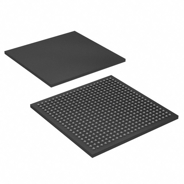
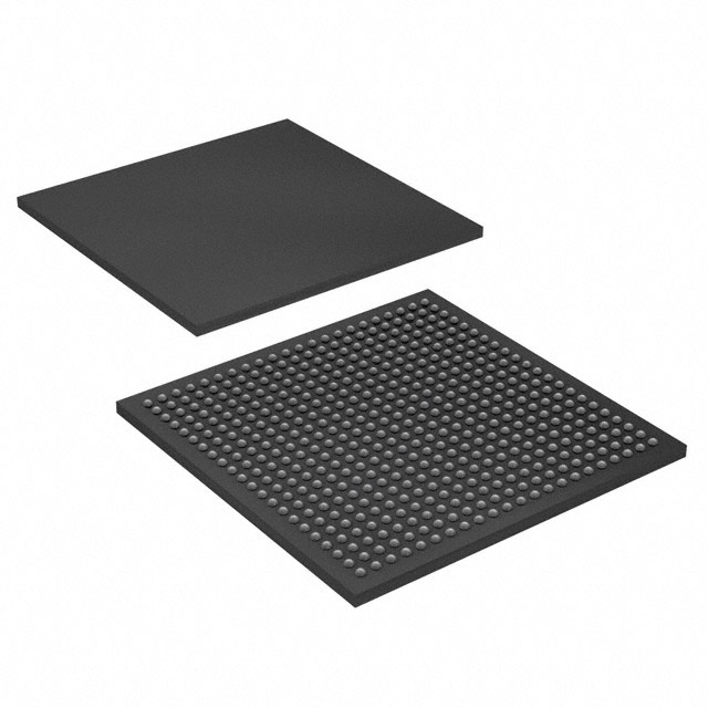
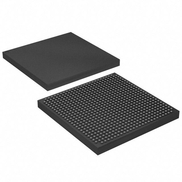
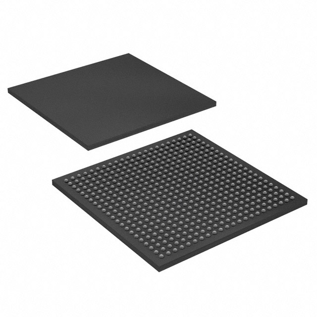
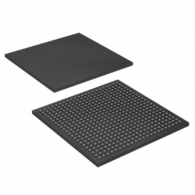
APEX-20KE® Field Programmable Gate Array (FPGA) IC 376 106496 8320 484-BBGA |
|---|---|
| Quantity | 639 Available (as of October 8, 2026) |
| Product Category | Field Programmable Gate Array (FPGA) |
|---|---|
| Manufacturer | Intel |
| Manufacturing Status | Obsolete |
| Manufacturer Standard Lead Time | Contact Us |
| Datasheet |
Specifications & Environmental
| Device Package | 484-FBGA (23x23) | Grade | Commercial | Operating Temperature | 0°C – 85°C | ||
|---|---|---|---|---|---|---|---|
| Package / Case | 484-BBGA | Number of I/O | 376 | Voltage | 1.71 V - 1.89 V | ||
| Mounting Method | Surface Mount | RoHS Compliance | Unknown | REACH Compliance | REACH Unaffected | ||
| Moisture Sensitivity Level | 3 (168 Hours) | Number of LABs/CLBs | 832 | Number of Logic Elements/Cells | 8320 | ||
| Number of Gates | 526000 | ECCN | 3A991D | HTS Code | 8542.39.0001 | ||
| Qualification | N/A | Total RAM Bits | 106496 |
Overview of EP20K200EFC484-2XN – APEX-20KE® FPGA, 8,320 logic elements, 106,496-bit RAM, 376 I/O, 484-BBGA
The EP20K200EFC484-2XN is an APEX-20K family field programmable gate array (FPGA) IC from Intel. It implements the family’s MultiCore architecture that integrates look-up table (LUT) logic, product-term logic and embedded memory to support register‑intensive and memory‑intensive functions.
With 8,320 logic elements, approximately 0.106 Mbits of embedded memory (106,496 bits), 376 user I/Os and a 484‑ball BGA package, this commercial‑grade device targets medium‑density custom logic and interface applications that require flexible I/O, on‑chip memory and configurable clocking.
Key Features
- Core Capacity — 8,320 logic elements and a maximum system gate count of 526,000 provide a medium-density programmable fabric for combinational and sequential logic.
- Embedded Memory — Approximately 0.106 Mbits of on‑chip RAM (106,496 bits) suitable for FIFOs, small buffers and scratch memory.
- I/O Count & Flexibility — 376 user I/O pins with MultiVolt I/O interface support (1.8 V, 2.5 V, 3.3 V and 5.0 V per family documentation) to interface with a wide range of external devices.
- Clocking & Timing — Family-level clock management features such as up to four PLLs, a low‑skew clock tree and multiple global clock signals support complex timing and clock domain control.
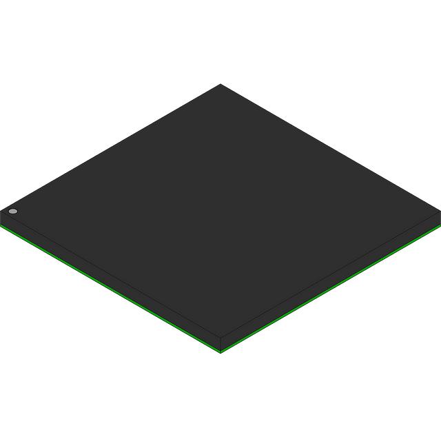
- Package & Mounting — 484‑BBGA package (supplier device package 484‑FBGA, 23×23) designed for surface‑mount assembly.
- Power — Core voltage supply specified at 1.71 V to 1.89 V for this part number; device family documentation also describes power‑saving and MultiVolt I/O capabilities.
- Operating Range — Commercial temperature grade with an operating range of 0 °C to 85 °C.
- Standards & Interfaces — Family documentation indicates support for high‑speed memory interfaces (including DDR SDRAM and ZBT SRAM), LVDS and PCI‑compliant operation for 3.3‑V PCI buses.
- Regulatory — RoHS compliant.
Typical Applications
- High‑speed memory interfaces — Implement DDR SDRAM or ZBT SRAM controllers and interface logic using the device’s embedded RAM and dedicated I/O support.
- PCI and bus bridge logic — Use the device’s PCI‑compliant I/O capabilities and flexible clocking for PCI/PCI‑like host or peripheral logic at 3.3 V.
- Communications and data lanes — Leverage LVDS and high‑speed I/O support for serial/parallel data channels and protocol bridging.
- Embedded system glue and peripheral control — Implement custom peripherals, protocol adapters and control logic that benefit from on‑chip RAM and multiple global clocks.
Unique Advantages
- Balanced integration: Combines LUT logic, product‑term logic and embedded memory in a single FPGA fabric to reduce external components and board complexity.
- Flexible I/O interfacing: 376 user I/Os and family MultiVolt support enable direct connectivity to a broad range of legacy and modern peripherals without additional level‑shifters.
- Configurable clocking: Multiple PLLs and a built‑in low‑skew clock tree simplify multi‑clock designs and help manage timing across clock domains.
- Appropriate density for mid‑range designs: 8,320 logic elements and ~106 Kbits of RAM provide capacity for medium‑complexity implementations while keeping board area and BOM under control.
- Commercial temperature and RoHS compliance: Clear environmental and regulatory positioning for mainstream electronic products and assemblies.
Why Choose EP20K200EFC484-2XN?
The EP20K200EFC484-2XN is positioned for designers who need a medium‑density, commercially graded FPGA with integrated memory, flexible I/O and mature family‑level clocking features. Its combination of 8,320 logic elements, 106,496 bits of embedded RAM and 376 I/Os in a 484‑ball BGA package makes it suitable for bridging, interface and embedded logic functions where on‑chip resources reduce external components.
Backed by the APEX‑20K family datasheet and Intel manufacturing, this device offers a documented set of architectural and I/O capabilities that support rapid integration into systems requiring DDR/ZBT memory interfaces, PCI signaling and high‑speed differential links.
Request a quote or submit a quote request to inquire about availability and pricing for EP20K200EFC484-2XN.





















Date Founded: 1968
Headquarters: Santa Clara, California, USA
Employees: 130,000+
Revenue: $54.23 Billion
Certifications and Memberships: ISO9001:2015, ISO14001:2015, ISO17025:2017, ISO27001:2022, ISO45001:2018, ISO50001:2018


