
EP20K200EFC672-1
| Part Description |
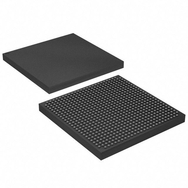
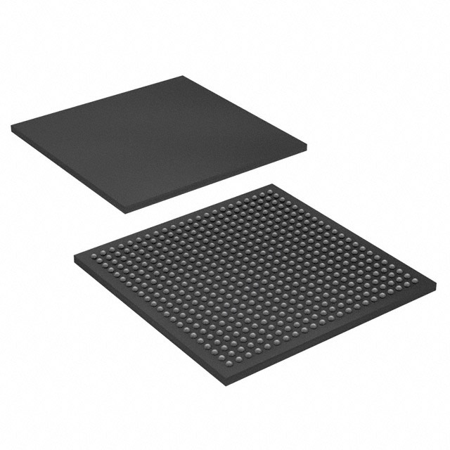
APEX-20KE® Field Programmable Gate Array (FPGA) IC 376 106496 8320 672-BBGA |
|---|---|
| Quantity | 25 Available (as of October 8, 2026) |
| Product Category | Field Programmable Gate Array (FPGA) |
|---|---|
| Manufacturer | Intel |
| Manufacturing Status | Obsolete |
| Manufacturer Standard Lead Time | Contact Us |
| Datasheet |
Specifications & Environmental
| Device Package | 672-FBGA (27x27) | Grade | Commercial | Operating Temperature | 0°C – 85°C | ||
|---|---|---|---|---|---|---|---|
| Package / Case | 672-BBGA | Number of I/O | 376 | Voltage | 1.71 V - 1.89 V | ||
| Mounting Method | Surface Mount | RoHS Compliance | RoHS non-compliant | REACH Compliance | REACH Unaffected | ||
| Moisture Sensitivity Level | 3 (168 Hours) | Number of LABs/CLBs | 832 | Number of Logic Elements/Cells | 8320 | ||
| Number of Gates | 526000 | ECCN | 3A991D | HTS Code | 8542.39.0001 | ||
| Qualification | N/A | Total RAM Bits | 106496 |
Overview of EP20K200EFC672-1 – APEX-20KE Field Programmable Gate Array, 672-BBGA
The EP20K200EFC672-1 is an Intel APEX-20KE series FPGA in a 672-ball BGA package designed for commercial-grade system integration. Built on the APEX MultiCore architecture, the device combines look-up table (LUT) logic, product-term logic and embedded memory blocks to address applications that require dense logic, embedded RAM and flexible I/O.
With 8,320 logic elements, approximately 0.106 Mbits of embedded memory and 376 user I/O pins, this device targets designs needing substantial logic capacity, on-chip memory and broad I/O support while operating from a low internal supply range.
Key Features
- Core Architecture MultiCore architecture integrating LUT logic, product-term logic and embedded system blocks (ESBs) for register‑intensive and combinatorial functions.
- Logic Capacity 8,320 logic elements and up to 526,000 system gates provide room for complex glue logic, state machines and custom processing engines.
- Embedded Memory Approximately 0.106 Mbits of on-chip RAM (106,496 bits) implemented as ESBs suitable for FIFOs, dual-port RAM and CAM functions.
- I/O and Interface Support 376 user I/O pins with MultiVolt™ I/O interface support for 1.8 V, 2.5 V, 3.3 V and 5.0 V signaling options and support for high-speed interfaces such as LVDS, PCI and DDR memory interconnects referenced in the device family documentation.
- Clocking and Timing Flexible clock management including up to four PLLs, a built-in low‑skew clock tree, up to eight global clock signals and programmable clock features (ClockLock, ClockBoost, ClockShift) for refined timing control.
- Power and I/O Control Designed for low-power operation with an internal supply voltage in the 1.71 V to 1.89 V range and programmable I/O slew-rate and clamp options to help manage switching noise and interface levels.
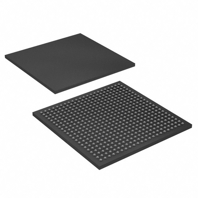
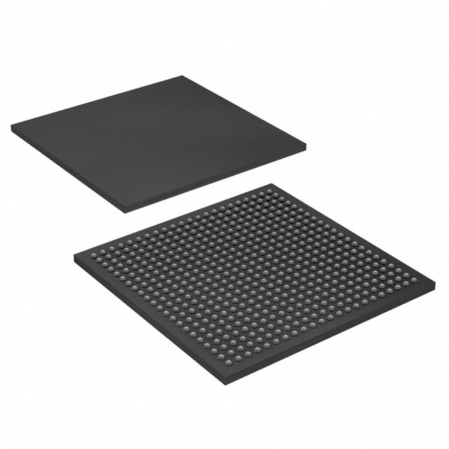
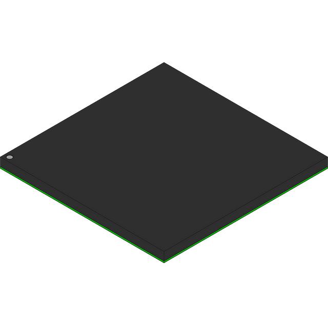
- Package and Mounting 672-BBGA package (supplier package: 672-FBGA, 27 × 27 mm) optimized for surface-mount assembly in space-constrained PCB layouts.
- Commercial Temperature Grade Rated for commercial operation from 0 °C to 85 °C.
- Standards and Compliance RoHS-compliant material status.
Typical Applications
- Memory Interface Controllers Implement DDR SDRAM and ZBT SRAM interfaces using the device’s high-speed I/O and ESB-based memory structures for buffering and protocol handling.
- High-speed Peripheral Bridging Bridge and translate between industry bus standards (for example PCI-level signaling scenarios documented for this device family) and custom logic domains.
- Custom Logic and Glue Replace legacy ASIC or discrete logic with reprogrammable logic for state machines, protocol offload and interface arbitration using 8,320 logic elements and plentiful I/O.
- Data Path and DSP Support Implement packet processing, serialization/deserialization, and medium-complexity datapath functions leveraging dedicated interconnect and product-term logic.
Unique Advantages
- MultiCore integration: Combines LUTs, product-term logic and embedded memory to consolidate multiple system functions into a single device, reducing board-level component count.
- Substantial on-chip memory: Approximately 0.106 Mbits of embedded RAM lets you implement FIFOs, buffers and small on-chip data stores without consuming logic resources.
- Flexible I/O voltages: MultiVolt I/O support simplifies interfacing to a wide range of legacy and modern signaling standards on the same board.
- Advanced clock management: Up to four PLLs, multiple global clocks and programmable clock features enable tight timing control for complex synchronous designs.
- Commercial-grade thermal range: Rated 0 °C to 85 °C for use in typical commercial embedded and communications equipment.
- Compact BGA packaging: 672-ball FBGA package provides high pin count in a compact 27 × 27 mm footprint for dense PCB designs.
Why Choose EP20K200EFC672-1?
The EP20K200EFC672-1 offers a balanced combination of logic density, on-chip memory and flexible I/O suitable for complex commercial embedded designs. Its MultiCore architecture and robust clocking features make it a practical choice for engineers consolidating multiple functions—memory interfaces, bus bridging and custom datapath logic—into a single programmable device.
For developers targeting compact, surface-mount solutions, the 672-BBGA package and comprehensive feature set provide scalability and integration while adhering to commercial operating conditions and RoHS compliance backed by Intel’s APEX 20K family documentation.
Request a quote or submit a purchasing inquiry to receive pricing, availability and delivery lead-time information for EP20K200EFC672-1.






















Date Founded: 1968
Headquarters: Santa Clara, California, USA
Employees: 130,000+
Revenue: $54.23 Billion
Certifications and Memberships: ISO9001:2015, ISO14001:2015, ISO17025:2017, ISO27001:2022, ISO45001:2018, ISO50001:2018


