
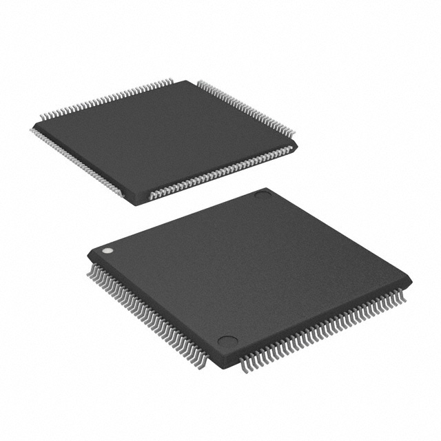
EP20K60ETC144-2X
| Part Description |
APEX-20KE® Field Programmable Gate Array (FPGA) IC 92 32768 2560 144-LQFP |
|---|---|
| Quantity | 1,944 Available (as of June 15, 2026) |

| Product Category | Field Programmable Gate Array (FPGA) |
|---|---|
| Manufacturer | Intel |
| Manufacturing Status | Obsolete |
| Manufacturer Standard Lead Time | Contact Us |
| Datasheet |
Specifications & Environmental
| Device Package | 144-TQFP (20x20) | Grade | Commercial | Operating Temperature | 0°C – 85°C | ||
|---|---|---|---|---|---|---|---|
| Package / Case | 144-LQFP | Number of I/O | 92 | Voltage | 1.71 V - 1.89 V | ||
| Mounting Method | Surface Mount | RoHS Compliance | Unknown | REACH Compliance | REACH Unaffected | ||
| Moisture Sensitivity Level | 3 (168 Hours) | Number of LABs/CLBs | 2560 | Number of Logic Elements/Cells | 2560 | ||
| Number of Gates | 162000 | ECCN | 3A001A2A | HTS Code | 8542.39.0001 | ||
| Qualification | N/A | Total RAM Bits | 32768 |
Overview of EP20K60ETC144-2X – APEX-20KE Field Programmable Gate Array, 144-LQFP
The EP20K60ETC144-2X is an APEX-20KE family FPGA in a 144-pin LQFP package designed for commercial embedded logic applications. Based on the APEX 20K family architecture, it combines lookup-table (LUT) logic and embedded system blocks (ESBs) to support register-intensive and memory-intensive functions. Typical use cases include control logic, custom peripherals, and mid-density system integration where deterministic logic resources, embedded RAM, and flexible I/O are required.
Key Features
- Core Architecture MultiCore family architecture integrating LUT logic and product-term logic for register- and combinatorial-intensive functions; device family-level architecture supports systematic SOPC-style integration.
- Logic Capacity 2,560 logic elements (LEs) providing a mid-density programmable logic resource; specified at 162,000 maximum system gates for the device variant.
- Embedded Memory 32,768 total RAM bits (approximately 32 Kbits) implemented in ESBs suitable for FIFOs, dual-port RAM and small on-chip buffers.
- I/O Resources 92 user I/O pins with family-level MultiVolt I/O support across common I/O voltage levels; I/O architecture includes features for programmable slew rate and individual tri-state control.
- Clocking and Timing Family-level clock management features such as up to four PLLs, a low-skew clock tree and multiple global clock signals enable deterministic clock distribution and phase control.
- Power and Voltage Designed for low-power operation with an internal supply range of 1.71 V to 1.89 V for this device variant; family features include power-saving modes in ESBs.
- Package and Mounting 144-LQFP package (supplier device package: 144-TQFP, 20×20) in a surface-mount form factor, simplifying PCB assembly for compact boards.
- Operating Conditions Commercial grade operation with an operating temperature range of 0 °C to 85 °C and RoHS-compliant materials.
Typical Applications
- Embedded Control Implement microcontroller-like peripherals, state machines and timing-critical control logic in mid-density embedded systems.
- Custom I/O and Protocol Bridging Develop interface logic and protocol converters that benefit from flexible I/O and MultiVolt support.
- On-board Memory Management Use ESBs for small FIFOs, buffering and dual-port RAM functions to offload simple memory tasks from external components.
- Prototyping and System Integration Mid-density FPGA capacity and a compact LQFP footprint make this device suitable for early system integration and prototype designs.
Unique Advantages
- Balanced Logic and Memory Mix: 2,560 logic elements combined with approximately 32 Kbits of embedded RAM allow compact implementations of both control logic and modest data buffering.
- Flexible I/O Support: 92 user I/O pins and family-level MultiVolt I/O enable direct interfacing with multiple logic voltage domains without complex level-shifting circuitry.
- Deterministic Clocking: Family clock-management features, including PLLs and a low-skew clock tree, simplify clock distribution and phase management for synchronous designs.
- Compact Surface-Mount Package: 144-LQFP (144-TQFP, 20×20) provides a compact footprint suited to tighter PCB layouts while remaining surface-mount assembler-friendly.
- RoHS-Compliant Commercial Grade: Commercial temperature range (0 °C to 85 °C) and RoHS compliance support standard commercial product lines and regulatory requirements.
Why Choose EP20K60ETC144-2X?
The EP20K60ETC144-2X offers a practical blend of mid-range logic capacity, on-chip RAM, and flexible I/O in a compact LQFP package for commercial embedded designs. Its APEX-20KE family architecture provides LUT-based logic and ESB-based memory resources that make it suitable for designs requiring both register-intensive and memory-centric functions.
This device is best for teams developing mid-density custom logic, protocol bridging, on-board buffering and prototype systems where predictable resources, commercial temperature operation, and a surface-mount LQFP footprint align with project requirements.
Request a quote or submit an RFQ today to check pricing and availability for the EP20K60ETC144-2X and assess its fit for your next design.


Date Founded: 1968
Headquarters: Santa Clara, California, USA
Employees: 130,000+
Revenue: $54.23 Billion
Certifications and Memberships: ISO9001:2015, ISO14001:2015, ISO17025:2017, ISO27001:2022, ISO45001:2018, ISO50001:2018


