
EP2A15B724C7
| Part Description |
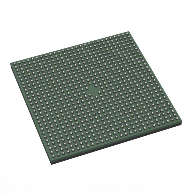
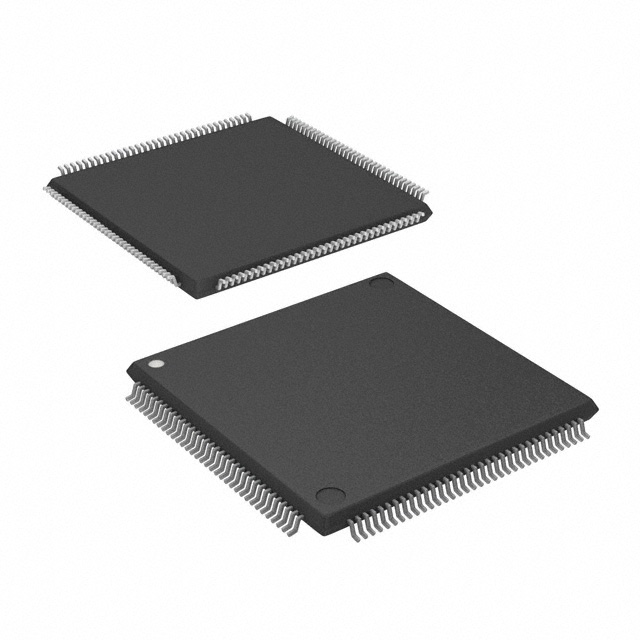
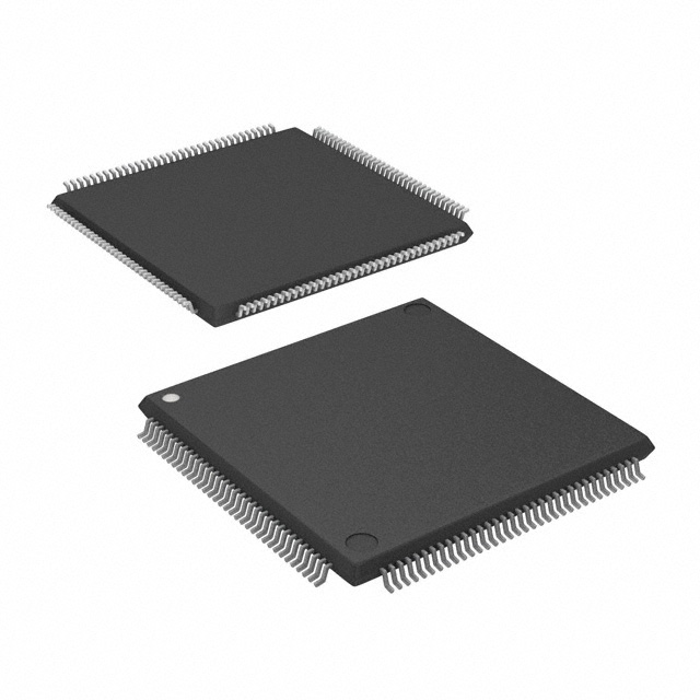
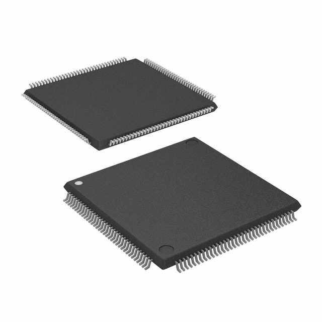
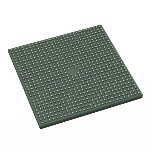
APEX II Field Programmable Gate Array (FPGA) IC 492 425984 16640 724-BBGA, FCBGA |
|---|---|
| Quantity | 305 Available (as of October 7, 2026) |
| Product Category | Field Programmable Gate Array (FPGA) |
|---|---|
| Manufacturer | Intel |
| Manufacturing Status | Obsolete |
| Manufacturer Standard Lead Time | Contact Us |
| Datasheet |
Specifications & Environmental
| Device Package | 724-BGA (35x35) | Grade | Commercial | Operating Temperature | 0°C – 85°C | ||
|---|---|---|---|---|---|---|---|
| Package / Case | 724-BBGA, FCBGA | Number of I/O | 492 | Voltage | 1.425 V - 1.575 V | ||
| Mounting Method | Surface Mount | RoHS Compliance | Unknown | REACH Compliance | REACH Unknown | ||
| Moisture Sensitivity Level | 3 (168 Hours) | Number of LABs/CLBs | 1664 | Number of Logic Elements/Cells | 16640 | ||
| Number of Gates | 1900000 | ECCN | 3A001A2C | HTS Code | 8542.39.0001 | ||
| Qualification | N/A | Total RAM Bits | 425984 |
Overview of EP2A15B724C7 – APEX II FPGA, 16,640 logic elements, ~0.426 Mbits RAM, 492 I/Os, 724‑BBGA (35×35)
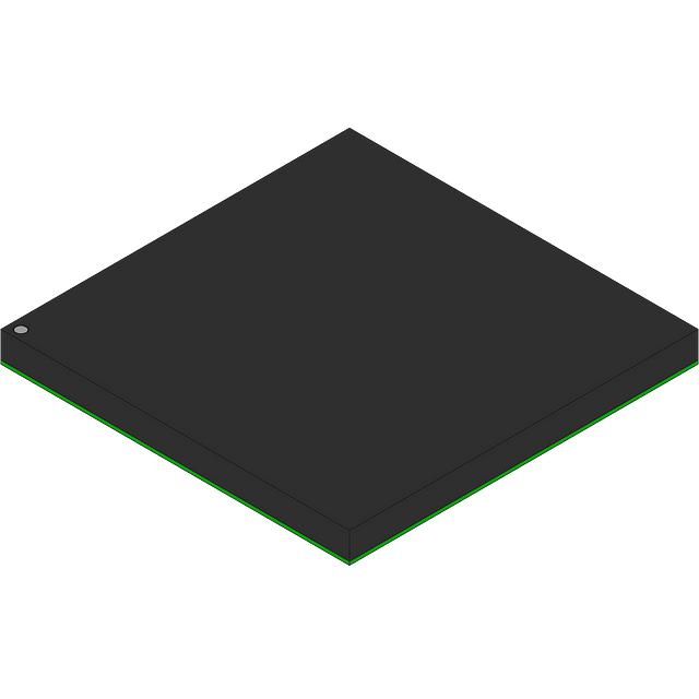
The EP2A15B724C7 is an APEX II family field-programmable gate array (FPGA) in a 724‑BBGA (35×35) FCBGA package. It provides a programmable logic fabric with 16,640 logic elements, approximately 0.426 Mbits of embedded RAM, and up to 492 user I/O pins for complex interface and system-integration tasks.
Designed for commercial applications that require high-density I/O, on‑chip memory, and flexible I/O standards, this device supports a range of high‑speed serial and parallel interfaces and offers a narrow core supply range for consistent operation across system designs.
Key Features
- Core Logic — 16,640 logic elements and approximately 1,900,000 system gates provide substantial programmable logic capacity for control, glue logic, and custom data-path implementations.
- Embedded Memory — Approximately 0.426 Mbits of on‑chip RAM with enhanced 4,096‑bit ESBs that support FIFO, Dual‑Port+ RAM and CAM functions for buffering and local storage.
- I/O Capacity & Standards — Up to 492 user I/O pins with MultiVolt I/O support for 1.5 V, 1.8 V, 2.5 V, and 3.3 V interfaces; supports high‑speed I/O modes and common networking standards documented for the APEX II family.
- High‑Speed Interface Support — Family-level support for 1 Gbps True‑LVDS, LVPECL, PCML and HyperTransport interfaces, plus flexible LVDS options for multi‑channel serial and parallel I/O applications.
- Performance & Interconnect — Fabric manufactured with a 0.15‑µm copper‑metal process and multiple metal layers to enable improved interconnect performance and lower power consumption.
- Power & Voltage — Nominal 1.5 V core operation with an explicitly specified supply range of 1.425 V to 1.575 V; copper interconnect and ESB power‑saving modes help manage power in system designs.
- Package & Mounting — 724‑BBGA (FCBGA) surface‑mount package, supplier device package 724‑BGA (35×35), suitable for compact board layouts requiring high I/O density.
- Operating Range & Compliance — Commercial grade with an operating temperature range of 0 °C to 85 °C and RoHS‑compliant construction.
Typical Applications
- High‑speed communications — Implement interface bridging, protocol conversion, and custom packet processing using the device’s high‑speed I/O and True‑LVDS/Flexible‑LVDS capabilities.
- Memory interface controllers — Build controllers for ZBT, QDR, DDR SRAM, and SDR/DDR SDRAM with on‑chip logic and embedded RAM for buffering and control state.
- PCI/PCI‑X subsystem logic — Use the programmable fabric to implement PCI or PCI‑X glue logic, bus adapters, and system control functions where 32/64‑bit or 33/66 MHz operation is required.
- Network and telecom equipment — Deploy in chassis or line card designs that require flexible I/O standards and substantial on‑chip memory for packet buffering or CAM‑style lookups.
Unique Advantages
- Significant programmable capacity: 16,640 logic elements and ~1.9M gates enable complex designs without external glue logic.
- On‑chip memory versatility: Approximately 0.426 Mbits of embedded RAM and 4,096‑bit ESBs support FIFOs, dual‑port RAM, and CAM implementations to reduce external memory needs.
- Broad I/O flexibility: Up to 492 I/Os and MultiVolt I/O support simplify integration with mixed‑voltage peripherals and high‑speed interface standards.
- Controlled power envelope: Nominal 1.5 V core operation with a defined supply window (1.425–1.575 V) and copper interconnect helps manage power in densely packed designs.
- Compact, high‑density package: 724‑BBGA (35×35) FCBGA packaging gives high I/O and logic density for space‑constrained PCBs.
- Commercial compliance and RoHS: Commercial operating range (0 °C to 85 °C) and RoHS compliance support standard commercial production and assembly processes.
Why Choose EP2A15B724C7?
The EP2A15B724C7 delivers a balance of mid‑range FPGA capacity, flexible high‑speed I/O, and on‑chip memory resources suitable for communications, memory-interface, and system‑integration tasks in commercial applications. Its APEX II family architecture and copper interconnect process provide a combination of logic density and power efficiency useful for designs that require substantial programmable logic with extensive I/O.
Ideal for engineering teams building compact subsystems, interface bridges, or buffering-intensive modules, this device provides verifiable specifications—logic elements, gate capacity, embedded RAM, I/O count, supply range, package, and operating temperature—to support planning, BOM decisions, and system validation.
Request a quote or submit an inquiry to receive pricing, availability, and lead‑time information for EP2A15B724C7.





















Date Founded: 1968
Headquarters: Santa Clara, California, USA
Employees: 130,000+
Revenue: $54.23 Billion
Certifications and Memberships: ISO9001:2015, ISO14001:2015, ISO17025:2017, ISO27001:2022, ISO45001:2018, ISO50001:2018


