
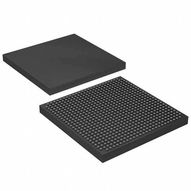
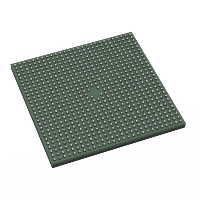
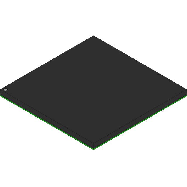
EP2A15F672C7
| Part Description |
APEX II Field Programmable Gate Array (FPGA) IC 492 425984 16640 672-BBGA |
|---|---|
| Quantity | 312 Available (as of June 14, 2026) |

| Product Category | Field Programmable Gate Array (FPGA) |
|---|---|
| Manufacturer | Intel |
| Manufacturing Status | Obsolete |
| Manufacturer Standard Lead Time | Contact Us |
| Datasheet |
Specifications & Environmental
| Device Package | 672-FBGA (27x27) | Grade | Commercial | Operating Temperature | 0°C – 85°C | ||
|---|---|---|---|---|---|---|---|
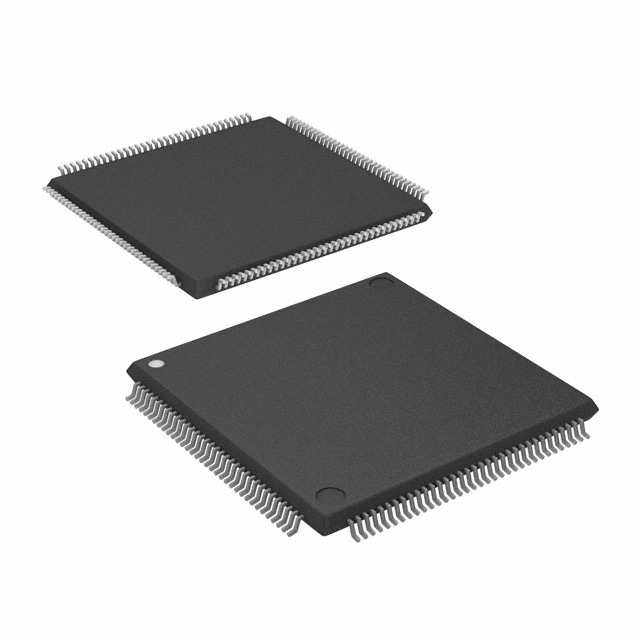
| Package / Case | 672-BBGA | Number of I/O | 492 | Voltage | 1.425 V - 1.575 V | ||
| Mounting Method | Surface Mount | RoHS Compliance | Unknown | REACH Compliance | REACH Unaffected | ||
| Moisture Sensitivity Level | 3 (168 Hours) | Number of LABs/CLBs | 1664 | Number of Logic Elements/Cells | 16640 | ||
| Number of Gates | 1900000 | ECCN | 3A001A2C | HTS Code | 8542.39.0001 | ||
| Qualification | N/A | Total RAM Bits | 425984 |
Overview of EP2A15F672C7 – APEX II Field Programmable Gate Array, 672‑BBGA
The EP2A15F672C7 is an APEX II family FPGA offering mid-range logic density and extensive high‑speed I/O. Built on a 0.15‑µm copper‑metal process, it targets communications, networking, memory‑interface, and custom logic applications that require a balance of logic resources, embedded memory, and multi‑standard I/O.
With 16,640 logic elements, 425,984 bits of on‑chip RAM, and 492 user I/Os in a compact 672‑BBGA package, this device delivers integrated I/O flexibility, embedded memory blocks, and configurable high‑speed interfaces for system designers.
Key Features
- Core Architecture 0.15‑µm all‑layer copper‑metal fabrication with up to eight metal layers for lower interconnect resistance and improved performance.
- Logic Resources 16,640 logic elements (LEs) and approximately 1,900,000 system gates provide mid‑range programmable logic capacity for complex designs.
- Embedded Memory Approximately 0.426 Mbits of on‑chip RAM implemented as enhanced 4,096‑bit ESBs supporting FIFO, Dual‑Port+ RAM, and CAM functions.
- I/O and High‑Speed Interfaces 492 user I/Os with dedicated support for 36 True‑LVDS channels and 56 Flexible‑LVDS channels. Supports 1‑Gbps True‑LVDS, LVPECL, PCML and HyperTransport interfaces and common networking standards such as RapidIO, CSIX, Utopia IV, and POS‑PHY Level 4 (as described for the APEX II family).
- Memory and Bus Support Architectural support for high‑speed external memories and interfaces including ZBT, QDR, DDR SRAM, SDR and DDR SDRAM, suitable for designs requiring fast external memory access.
- Clocking and PLLs Dedicated True‑LVDS PLLs and general‑purpose PLL outputs (four True‑LVDS PLLs and eight general outputs in the APEX II EP2A15 family configuration) to support clock multiplication, deskewing, and serialization/deserialization.
- Power and I/O Voltage Core supply range 1.425 V to 1.575 V. MultiVolt I/O support across common interface voltages enables integration with various external logic levels.
- Package and Mounting Surface‑mount 672‑BBGA package (supplier device package 672‑FBGA, 27×27 mm) for high I/O density in a compact footprint.
- Operating Conditions and Compliance Commercial grade operation from 0 °C to 85 °C. RoHS‑compliant manufacturing.
Typical Applications
- Networking & Communications Implements protocol bridging, packet processing, and I/O aggregation using True‑LVDS and Flexible‑LVDS channels plus support for RapidIO and related standards.
- High‑Speed Memory Interfaces Acts as a programmable controller or buffer for ZBT/QDR/DDR SRAM and SDR/DDR SDRAM in systems requiring deterministic memory access.
- Serial and Parallel Interface Bridging Enables serialization/deserialization and clock‑data synchronization for multi‑Gbps links, leveraging dedicated PLLs and clock‑synchronization circuitry.
- Custom Logic and Prototyping Provides a flexible platform for implementing custom state machines, data path logic, and hardware acceleration with substantial on‑chip RAM and LEs.
Unique Advantages
- Balanced Logic and Memory 16,640 LEs combined with approximately 425,984 bits of embedded RAM provide room for logic‑heavy designs that also need local storage and FIFOs.
- High I/O Count 492 user I/Os support dense external connectivity and parallel interfaces without external multiplexing hardware.
- Multi‑Standard High‑Speed I/O Native support for True‑LVDS, LVPECL, PCML and HyperTransport interfaces simplifies integration with contemporary communications and host interfaces.
- Dedicated Clocking Resources Multiple PLL outputs and True‑LVDS PLLs enable robust clock management for high‑speed serial links and synchronized data transfers.
- Compact, High‑Density Package 672‑BBGA (672‑FBGA, 27×27 mm) delivers high I/O and logic density in a space‑efficient form factor for board‑level integration.
- Regulatory and Manufacturing Readiness RoHS compliance and surface‑mount packaging facilitate modern manufacturing and environmental requirements.
Why Choose EP2A15F672C7?
The EP2A15F672C7 from the APEX II family combines a mid‑range logic fabric with substantial embedded memory and a broad set of high‑speed I/O capabilities. Its combination of 16,640 logic elements, approximately 425,984 bits of on‑chip RAM, 492 I/Os, and dedicated PLL resources makes it well suited to communications, memory‑interface, and custom logic applications that require integrated high‑speed interfaces and clocking flexibility.
Designed for commercial temperature operation and available in a compact 672‑BBGA package, the EP2A15F672C7 is a practical choice for system designers seeking a programmable device that balances logic capacity, embedded memory, and multi‑standard I/O support within the APEX II architecture.
Request a quote or submit a pricing and availability inquiry to begin evaluation and procurement of EP2A15F672C7 for your next design.


Date Founded: 1968
Headquarters: Santa Clara, California, USA
Employees: 130,000+
Revenue: $54.23 Billion
Certifications and Memberships: ISO9001:2015, ISO14001:2015, ISO17025:2017, ISO27001:2022, ISO45001:2018, ISO50001:2018


