
EP2A15B724C9
| Part Description |
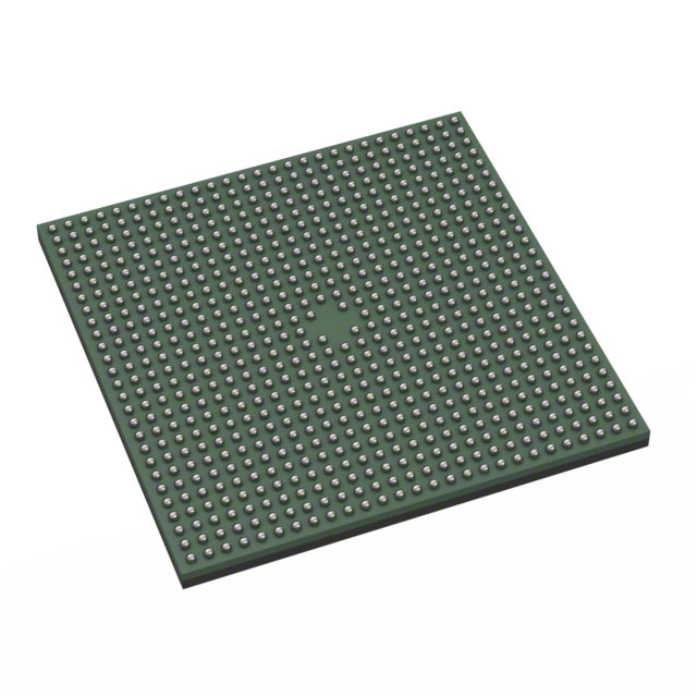
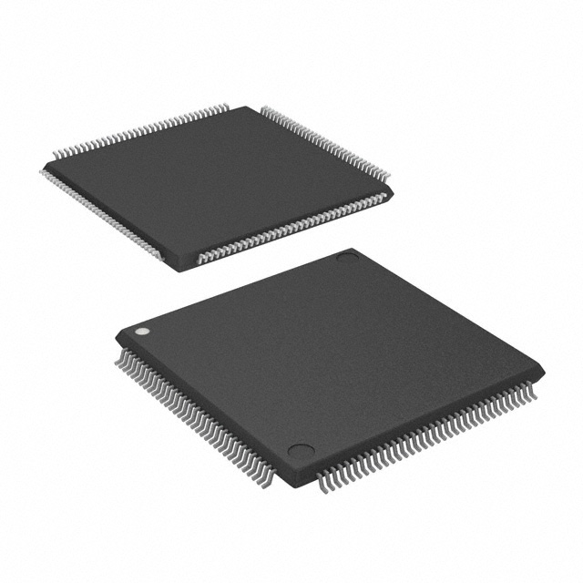
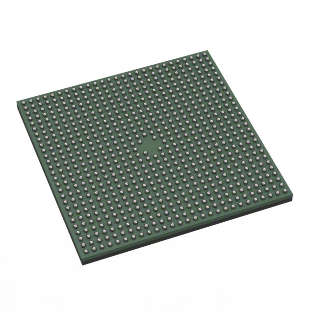
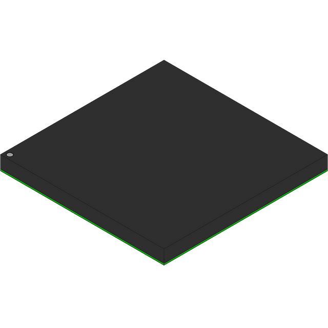
APEX II Field Programmable Gate Array (FPGA) IC 492 425984 16640 724-BBGA, FCBGA |
|---|---|
| Quantity | 208 Available (as of October 7, 2026) |
| Product Category | Field Programmable Gate Array (FPGA) |
|---|---|
| Manufacturer | Intel |
| Manufacturing Status | Obsolete |
| Manufacturer Standard Lead Time | Contact Us |
| Datasheet |
Specifications & Environmental
| Device Package | 724-BGA (35x35) | Grade | Commercial | Operating Temperature | 0°C – 85°C | ||
|---|---|---|---|---|---|---|---|
| Package / Case | 724-BBGA, FCBGA | Number of I/O | 492 | Voltage | 1.425 V - 1.575 V | ||
| Mounting Method | Surface Mount | RoHS Compliance | Unknown | REACH Compliance | REACH Unknown | ||
| Moisture Sensitivity Level | 3 (168 Hours) | Number of LABs/CLBs | 1664 | Number of Logic Elements/Cells | 16640 | ||
| Number of Gates | 1900000 | ECCN | 3A001A2C | HTS Code | 8542.39.0001 | ||
| Qualification | N/A | Total RAM Bits | 425984 |
Overview of EP2A15B724C9 – APEX II Field Programmable Gate Array (FPGA) IC, 724-BBGA (35×35)
The EP2A15B724C9 is an APEX II family Field Programmable Gate Array (FPGA) in a 724-BBGA FCBGA package (724-BGA, 35×35). It delivers a balance of on-chip logic, embedded memory, and high-density I/O to support communications, high-speed memory interfaces, and system integration tasks.
With 16,640 logic elements, approximately 0.426 Mbits of embedded memory, and 492 user I/Os, this commercial-grade, RoHS-compliant device targets applications that require flexible I/O standards, multi-protocol interfacing, and scalable programmable logic within a 0 °C to 85 °C operating range.
Key Features
- Core Logic 16,640 logic elements and approximately 1,900,000 system gates provide significant capacity for custom digital logic and control functions.
- Embedded Memory Approximately 0.426 Mbits of on-chip RAM (425,984 total RAM bits) with enhanced 4,096-bit ESBs supporting FIFO, Dual-Port+ RAM and CAM configurations.
- I/O Density & High-Speed Interfaces 492 user I/O pins with support for True-LVDS and Flexible-LVDS channels (36 True-LVDS channels, 56 Flexible-LVDS channels) and a family capability of up to 380 Gbps of I/O throughput for demanding interface tasks.
- Interoperability & Standards Architecture supports common networking and communications bus standards and high-speed external memory interfaces including ZBT, QDR, DDR SRAM, SDR and DDR SDRAM (series-level features documented in the APEX II family datasheet).
- Power & Voltage Core voltage supply specified at 1.425 V to 1.575 V; family-level features include low-power copper interconnect and MultiVolt I/O support for multiple I/O voltage levels.
- Package & Mounting 724-BBGA (FCBGA) surface-mount package, supplier device package listed as 724-BGA (35×35), suitable for compact board layouts.
- Commercial Grade & Environmental Commercial-grade device with operating temperature range 0 °C to 85 °C and RoHS compliance.
Typical Applications
- Networking & Communications High-density I/O and True-LVDS/Flexible-LVDS support enable implementation of interfaces and protocol bridging for networking equipment and telecom modules.
- High-Speed Memory Controllers Support for ZBT, QDR and DDR/SDR external memory interfaces makes the device suitable for custom memory controller and buffer designs.
- Interface Bridging & Protocol Translation Rich I/O capability and programmable logic density allow designers to implement protocol converters, serialization/deserialization, and custom interface logic.
- System Prototyping & Integration The combination of logic elements, embedded memory, and abundant I/O makes the FPGA well suited for prototyping and integrating digital subsystems on compact boards.
Unique Advantages
- Substantial logic capacity: 16,640 logic elements deliver ample programmable resources for mid-density designs without immediate need to move to larger device families.
- Significant on-chip RAM: Approximately 0.426 Mbits of embedded memory, including 4,096-bit ESBs, supports FIFOs, dual-port RAM, and CAM implementations to reduce external memory dependence.
- High I/O count with high-speed options: 492 user I/Os plus family-level True-LVDS and Flexible-LVDS channels enable high-throughput, multi-standard interfaces in a single device.
- Compact, high-density package: 724-BBGA (35×35) FCBGA footprint allows integration into space-constrained designs while providing extensive I/O and routing density.
- Commercial-grade reliability: Designed for 0 °C to 85 °C operation and RoHS compliance for mainstream electronics and embedded systems.
Why Choose EP2A15B724C9?
The EP2A15B724C9 offers a balanced combination of programmable logic, embedded memory, and dense I/O in a compact 724-BBGA package, making it a practical choice for communications, memory interface, and system integration designs that require mid-range logic capacity. Its inclusion in the APEX II family means designers can leverage family-level features documented in the datasheet—including high-speed I/O options and flexible memory interfaces—while matching device size to application needs.
Designed for commercial applications and backed by APEX II family documentation, the EP2A15B724C9 suits engineering teams needing scalable programmable logic with verified electrical characteristics (1.425 V to 1.575 V core supply) and defined operating temperature limits for reliable deployment in mainstream embedded products.
Request a quote or submit a purchase inquiry for EP2A15B724C9 to receive pricing and availability information tailored to your project requirements.





















Date Founded: 1968
Headquarters: Santa Clara, California, USA
Employees: 130,000+
Revenue: $54.23 Billion
Certifications and Memberships: ISO9001:2015, ISO14001:2015, ISO17025:2017, ISO27001:2022, ISO45001:2018, ISO50001:2018


