
EP2A15F672C7N
| Part Description |
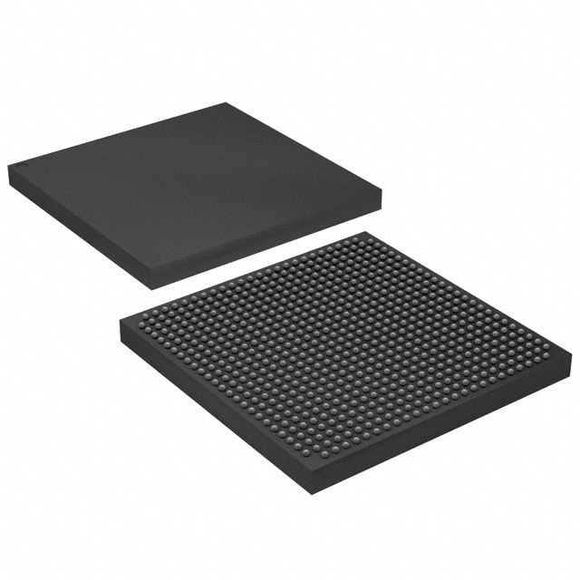
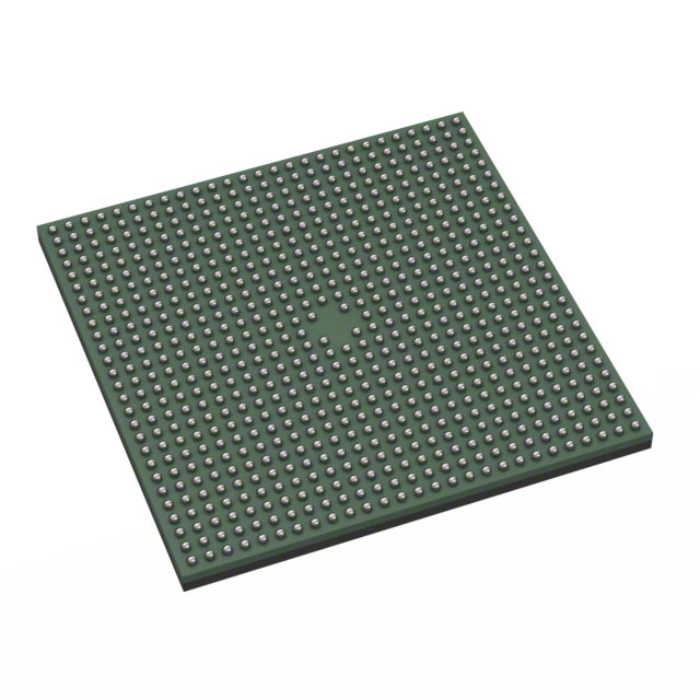
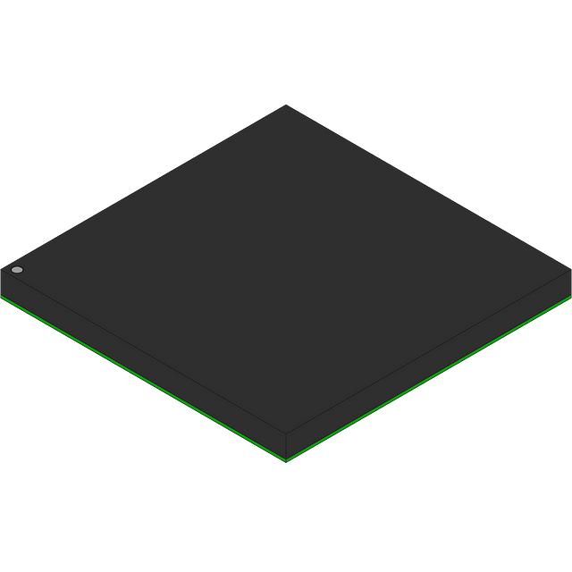
APEX II Field Programmable Gate Array (FPGA) IC 492 425984 16640 672-BBGA |
|---|---|
| Quantity | 950 Available (as of October 8, 2026) |
| Product Category | Field Programmable Gate Array (FPGA) |
|---|---|
| Manufacturer | Intel |
| Manufacturing Status | Obsolete |
| Manufacturer Standard Lead Time | Contact Us |
| Datasheet |
Specifications & Environmental
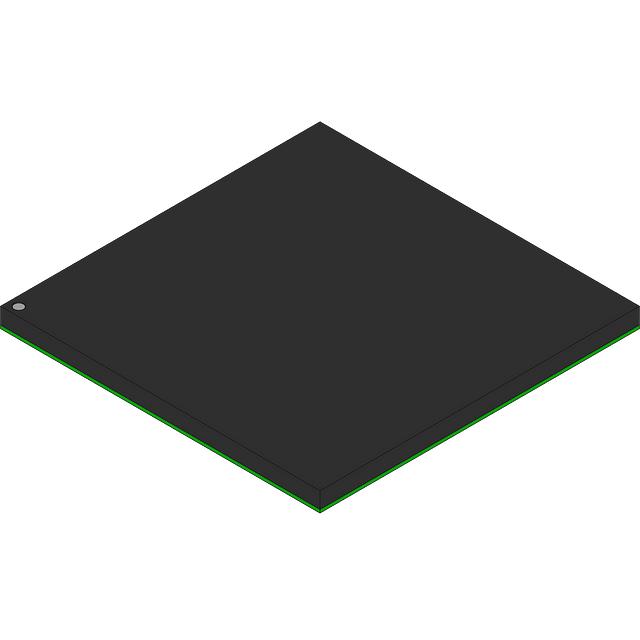
| Device Package | 672-FBGA (27x27) | Grade | Commercial | Operating Temperature | 0°C – 85°C | ||
|---|---|---|---|---|---|---|---|
| Package / Case | 672-BBGA | Number of I/O | 492 | Voltage | 1.425 V - 1.575 V | ||
| Mounting Method | Surface Mount | RoHS Compliance | Unknown | REACH Compliance | REACH Unaffected | ||
| Moisture Sensitivity Level | 3 (168 Hours) | Number of LABs/CLBs | 1664 | Number of Logic Elements/Cells | 16640 | ||
| Number of Gates | 1900000 | ECCN | 3A001A2C | HTS Code | 8542.39.0001 | ||
| Qualification | N/A | Total RAM Bits | 425984 |
Overview of EP2A15F672C7N – APEX II Field Programmable Gate Array (FPGA) IC 672-BBGA
The EP2A15F672C7N is an APEX II family programmable logic device from Intel, delivering mid-range FPGA capacity and high‑performance I/O for communications and embedded designs. Built on the APEX II architecture, it combines a substantial logic fabric with dedicated memory blocks and multi-standard I/O to address networking, high‑speed memory interfaces, and general-purpose embedded applications.
With 16,640 logic elements, up to 1,900,000 system gates, and extensive I/O capability, this commercial‑grade device targets designs that require flexible interfacing, on‑chip buffering, and deterministic clocking within a 672‑ball BGA footprint.
Key Features
- Core Capacity 16,640 logic elements and approximately 1,900,000 maximum system gates provide substantial programmable logic for mid-density designs.
- On‑chip Memory Approximately 0.426 Mbits of embedded memory (total RAM bits: 425,984) and 104 enhanced 4,096‑bit ESBs for FIFOs, Dual‑Port+ RAM and CAM functions.
- I/O and High‑Speed Interfaces Up to 492 user I/O pins with support in the APEX II family for 1‑Gbps True‑LVDS, LVPECL, PCML and HyperTransport interfaces; 36 True‑LVDS channels and 56 Flexible‑LVDS channels for synchronous, multi‑lane links.
- Clocking and PLLs Dedicated True‑LVDS PLL resources and general‑purpose PLL outputs (family table: 4 True‑LVDS PLLs, 8 general‑purpose PLL outputs) for independent clock multiplication, deskew and serialization/deserialization.
- Memory Interface Support Family-level support for high‑speed external memory interfaces including ZBT, QDR and DDR SRAM, SDR and DDR SDRAM (series data sheet).
- Power and Packaging Supply voltage range 1.425 V to 1.575 V; surface‑mount 672‑BBGA package (supplier device package listed as 672‑FBGA 27×27) suitable for compact board designs.
- Operating Conditions and Compliance Commercial operating temperature range 0 °C to 85 °C and RoHS compliant for environmental regulation alignment.
Typical Applications
- High‑speed Networking Use the device’s True‑LVDS and Flexible‑LVDS channels and dense I/O to implement multi‑lane links, protocol bridging, and packet processing functions.
- Memory Interface Controllers Implement controllers and interface logic for ZBT, QDR and DDR memory technologies leveraging the on‑chip ESBs and dedicated clocking resources.
- Telecommunications Equipment Deploy in telecom line cards and switching modules where deterministic clocking, embedded FIFOs, and multi‑standard I/O are required.
- Commercial Embedded Systems Integrate for system control, data aggregation, and custom hardware acceleration in commercial embedded products.
Unique Advantages
- Balanced Logic-to-Memory Ratio: 16,640 logic elements paired with approximately 0.426 Mbits of embedded memory supports logic‑intensive designs that also require substantial on‑chip buffering and storage.
- Robust I/O Versatility: Up to 492 I/O pins and multiple LVDS channel types enable flexible interfacing across high‑speed serial links and legacy parallel buses, reducing external translation components.
- Dedicated Clocking Resources: True‑LVDS PLLs and multiple PLL outputs allow precise clock management for serial links and memory interfaces, simplifying timing closure.
- Compact, Surface‑Mount Packaging: 672‑ball BGA footprint (27×27 supplier FBGA) provides a high‑density solution for space-constrained PCBs while supporting standard surface‑mount assembly.
- Commercial Temperature and RoHS Compliance: Rated for 0 °C to 85 °C operation and RoHS compliant for deployment in commercial products and regulated markets.
Why Choose EP2A15F672C7N?
The EP2A15F672C7N positions itself as a scalable, mid‑density APEX II FPGA option that balances programmable logic, embedded memory, and extensive I/O for communications and embedded designs. Its combination of 16,640 logic elements, dedicated ESBs, True‑LVDS/Flexible‑LVDS channel support and multiple PLL resources makes it well suited for applications that need reliable timing, multi‑standard interfacing, and on‑chip buffering in a compact BGA package.
As part of the APEX II family, designers can leverage family scalability and the series’ documented support for high‑speed memory and networking interfaces to match device capacity to application requirements while maintaining consistent design flows and board‑level integration.
Request a quote for EP2A15F672C7N to check availability and pricing, or submit a quote request to begin the procurement process for your next design.





















Date Founded: 1968
Headquarters: Santa Clara, California, USA
Employees: 130,000+
Revenue: $54.23 Billion
Certifications and Memberships: ISO9001:2015, ISO14001:2015, ISO17025:2017, ISO27001:2022, ISO45001:2018, ISO50001:2018


