
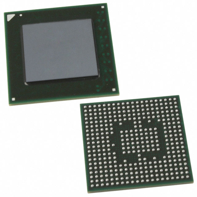
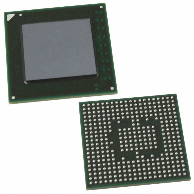
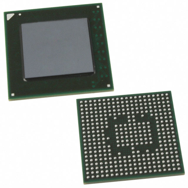
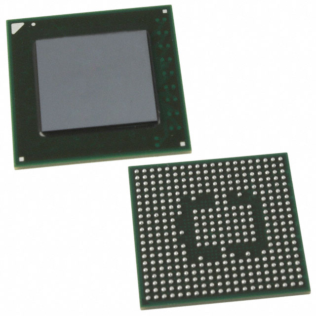
EP2AGX45CU17I3G
| Part Description |
Arria II GX Field Programmable Gate Array (FPGA) IC 156 3517440 42959 358-LFBGA, FCBGA |
|---|---|
| Quantity | 774 Available (as of October 8, 2026) |

| Product Category | Field Programmable Gate Array (FPGA) |
|---|---|
| Manufacturer | Intel |
| Manufacturing Status | Active |
| Manufacturer Standard Lead Time | 26 Weeks |
| Datasheet |
Specifications & Environmental
| Device Package | 358-UBGA, FCBGA (17x17) | Grade | Industrial | Operating Temperature | -40°C – 100°C | ||
|---|---|---|---|---|---|---|---|
| Package / Case | 358-LFBGA, FCBGA | Number of I/O | 156 | Voltage | 870 mV - 930 mV | ||
| Mounting Method | Surface Mount | RoHS Compliance | RoHS Compliant | REACH Compliance | REACH Unaffected | ||
| Moisture Sensitivity Level | 3 (168 Hours) | Number of LABs/CLBs | 1805 | Number of Logic Elements/Cells | 42959 | ||
| Number of Gates | N/A | ECCN | 3A991D | HTS Code | 8542.39.0001 | ||
| Qualification | N/A | Total RAM Bits | 3517440 |
Overview of EP2AGX45CU17I3G – Arria II GX FPGA, 358-LFBGA (FCBGA), Industrial
The EP2AGX45CU17I3G is an Arria II GX field programmable gate array (FPGA) in a 358-LFBGA (FCBGA) package, offered for industrial-grade applications. It delivers a 40‑nm, low‑power FPGA architecture intended for designs that require substantial logic capacity, embedded memory, and flexible I/O in a surface-mount BGA package.
Targeted at high-bandwidth interfaces, digital signal processing, and system integration tasks, the device combines approximately 42,959 logic elements with roughly 3.5 Mbits of on‑chip RAM and 156 user I/Os, providing a compact, production-ready FPGA option for industrial environments.
Key Features
- Core architecture 40‑nm Arria II family FPGA engine designed for low power and programmable logic integration.
- Logic capacity Approximately 42,959 logic elements suitable for mid‑to‑high complexity designs.
- Embedded memory Approximately 3.5 Mbits of on‑chip RAM to implement FIFOs, buffers, and local storage.
- I/O and integration 156 user I/O pins in a modular package format to support a range of single‑ended and differential interfaces.
- Package and mounting 358‑LFBGA (FCBGA) surface‑mount package; supplier device package listed as 358‑UBGA (17×17).
- Industrial temperature range Specified for −40 °C to 100 °C operation to meet demanding environmental requirements.
- Voltage supply Operating supply range of 870 mV to 930 mV as specified.
- Standards and compliance RoHS compliant for environmental and manufacturing conformity.
- Family-level transceiver and DSP capability As part of the Arria II family, the device benefits from family features such as up to 24 full‑duplex CDR‑based transceivers (600 Mbps to 6.375 Gbps) and high‑performance DSP blocks suitable for complex signal processing (refer to Arria II family documentation for full details).
Typical Applications
- Networking & Communications Implement PHY/MAC interfaces, high‑speed serial links and protocol bridging where compact FPGA logic and industrial temperature range are required.
- High‑performance Signal Processing Use embedded DSP resources and on‑chip RAM for filters, transforms, and real‑time data paths in communications and instrumentation equipment.
- Storage and Interface Controllers Deploy PCIe, SATA and other serial protocol endpoint or bridging logic leveraging the Arria II family’s PHY support and programmable fabric.
- Industrial Control and Automation Integrate sensor interfacing, motor control logic, and deterministic I/O handling within an industrial‑rated FPGA package.
Unique Advantages
- Significant logic density: Approximately 42,959 logic elements provide capacity for multi‑function designs without external glue logic.
- On‑chip memory for deterministic buffering: Approximately 3.5 Mbits of embedded RAM allow local buffering and low‑latency FIFOs that simplify system architecture.
- Industrial operating range: Rated from −40 °C to 100 °C to support deployment in a wide variety of industrial environments.
- Compact BGA packaging: 358‑LFBGA (FCBGA) surface‑mount package balances I/O count and board area for space‑constrained systems.
- Arria II family ecosystem: Access to family‑level transceiver, DSP and interface features and documentation for easier integration into high‑bandwidth systems.
- Regulatory readiness: RoHS compliance supports environmentally conscious production and assembly processes.
Why Choose EP2AGX45CU17I3G?
The EP2AGX45CU17I3G positions itself as a practical, industrial‑rated FPGA choice that combines mid‑range logic capacity, embedded memory, and a robust operating temperature range in a compact 358‑LFBGA package. Its Arria II family heritage brings proven transceiver and DSP features to designs that need reliable, programmable logic alongside interface flexibility.
This device is well suited for engineering teams building industrial communications, signal processing, and embedded control systems that require verifiable operating limits, on‑chip memory, and a solid FPGA ecosystem for integration and development.
Request a quote or submit an inquiry to receive pricing and availability for EP2AGX45CU17I3G and to discuss volume requirements or delivery timelines.























Date Founded: 1968
Headquarters: Santa Clara, California, USA
Employees: 130,000+
Revenue: $54.23 Billion
Certifications and Memberships: ISO9001:2015, ISO14001:2015, ISO17025:2017, ISO27001:2022, ISO45001:2018, ISO50001:2018


