
EP2AGX45DF25C5G
| Part Description |
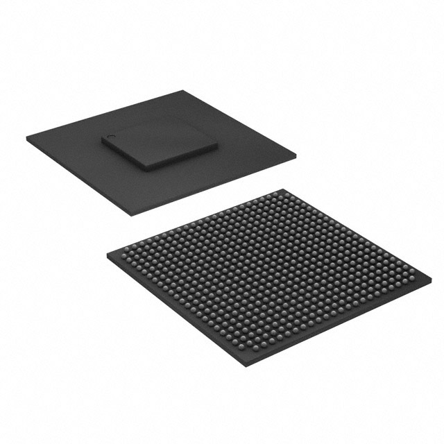
Arria II GX Field Programmable Gate Array (FPGA) IC 252 3517440 42959 572-BGA, FCBGA |
|---|---|
| Quantity | 822 Available (as of June 15, 2026) |

| Product Category | Field Programmable Gate Array (FPGA) |
|---|---|
| Manufacturer | Intel |
| Manufacturing Status | Active |
| Manufacturer Standard Lead Time | 26 Weeks |
| Datasheet |
Specifications & Environmental
| Device Package | 572-FBGA, FC (25x25) | Grade | Commercial | Operating Temperature | 0°C – 85°C | ||
|---|---|---|---|---|---|---|---|
| Package / Case | 572-BGA, FCBGA | Number of I/O | 252 | Voltage | 870 mV - 930 mV | ||
| Mounting Method | Surface Mount | RoHS Compliance | RoHS Compliant | REACH Compliance | REACH Unaffected | ||
| Moisture Sensitivity Level | 3 (168 Hours) | Number of LABs/CLBs | 1805 | Number of Logic Elements/Cells | 42959 | ||
| Number of Gates | N/A | ECCN | 3A991D | HTS Code | 8542.39.0001 | ||
| Qualification | N/A | Total RAM Bits | 3517440 |
Overview of EP2AGX45DF25C5G – Arria II GX FPGA, 42,959 Logic Elements, ~3.5 Mbits RAM, 252 I/O, 572-FBGA
The EP2AGX45DF25C5G is an Arria II GX field-programmable gate array (FPGA) in a 572‑FBGA surface-mount package. It combines a 40‑nm, low‑power FPGA engine from the Arria II family with a mid‑range logic capacity and on‑chip RAM suitable for complex interface and signal-processing tasks.
This device addresses applications that require moderate logic density, substantial embedded memory, and flexible I/O in a commercial‑temperature FPGA. The Arria II family architecture streamlines implementation of common high‑bandwidth interfaces and DSP functions, enabling faster integration of PCIe, Ethernet, DDR3 and other system interfaces when used with family design tools and IP.
Key Features
- Core Architecture 40‑nm Arria II family FPGA engine optimized for low power and efficient logic implementation.
- Logic Capacity 42,959 logic elements for implementing complex custom logic and control functions.
- Embedded Memory Approximately 3.5 Mbits of on‑chip RAM to support buffering, FIFOs, and local data storage.
- I/O and Package 252 user I/O pins in a 572‑FBGA (25 × 25 mm) surface‑mount package for compact, high‑density board designs.
- Power Nominal supply range from 870 mV to 930 mV to match system power rails and design constraints.
- Operating Conditions & Compliance Commercial grade operation from 0 °C to 85 °C; RoHS compliant.
- Family-Level Interfaces and Integration Arria II family features include streamlined transceivers and I/O for high‑bandwidth protocols, DSP blocks, and a broad IP/software design flow for implementing PCIe, Ethernet, DDR3 and similar interfaces.
Typical Applications
- High‑bandwidth Networking Implement Ethernet packet processing, protocol bridging, and interface control leveraging the Arria II family’s high‑speed interface support.
- Real‑time Signal Processing Use embedded RAM and DSP resources to implement filtering, FFTs, and data aggregation in communications or test equipment.
- Storage and Interface Controllers Deploy as a custom interface engine for storage protocols and host controller logic requiring moderate logic density and flexible I/O.
- Custom Logic and Prototyping Integrate control, glue logic, and bespoke accelerators where a commercial‑temperature FPGA with significant on‑chip memory is required.
Unique Advantages
- Substantial Logic Resource: 42,959 logic elements enable implementation of sophisticated state machines, datapaths, and control logic without immediate need for external processors.
- On‑Chip Memory for Local Data Handling: Approximately 3.5 Mbits of embedded RAM reduce dependence on external memory for buffering and small‑FIFO requirements.
- Compact, High‑Density Package: 572‑FBGA (25 × 25 mm) provides a balance of I/O count and board space for medium‑density system designs.
- Design Flow and IP Ecosystem: As part of the Arria II family, the device benefits from family design resources and IP for common interfaces, easing integration into larger systems.
- Commercial Temperature and RoHS Compliance: Rated 0 °C to 85 °C and RoHS compliant for mainstream electronic products and assemblies.
- Low‑Voltage Operation: Operates within an 870 mV to 930 mV supply window to match modern board power domains.
Why Choose EP2AGX45DF25C5G?
The EP2AGX45DF25C5G delivers a balanced combination of logic capacity, embedded memory, and flexible I/O in a compact 572‑FBGA package, making it well suited for designs that need moderate-density FPGA resources and reliable commercial‑temperature operation. As an Arria II GX device, it leverages family-level architecture and design resources that simplify implementation of high‑bandwidth system interfaces and signal‑processing functions.
This part is appropriate for engineering teams developing networking, storage interface, or signal‑processing applications that require integrated logic and memory while maintaining a small board footprint and standard commercial operating range.
Request a quote or submit an inquiry to get pricing and availability for EP2AGX45DF25C5G.


Date Founded: 1968
Headquarters: Santa Clara, California, USA
Employees: 130,000+
Revenue: $54.23 Billion
Certifications and Memberships: ISO9001:2015, ISO14001:2015, ISO17025:2017, ISO27001:2022, ISO45001:2018, ISO50001:2018


