
EP2AGX45DF25C4N
| Part Description |
Arria II GX Field Programmable Gate Array (FPGA) IC 252 3517440 42959 572-BGA, FCBGA |
|---|---|
| Quantity | 616 Available (as of June 14, 2026) |
| Product Category | Field Programmable Gate Array (FPGA) |
|---|---|
| Manufacturer | Intel |
| Manufacturing Status | Obsolete |
| Manufacturer Standard Lead Time | Contact Us |
| Datasheet |
Specifications & Environmental
| Device Package | 572-FBGA, FC (25x25) | Grade | Commercial | Operating Temperature | 0°C – 85°C | ||
|---|---|---|---|---|---|---|---|
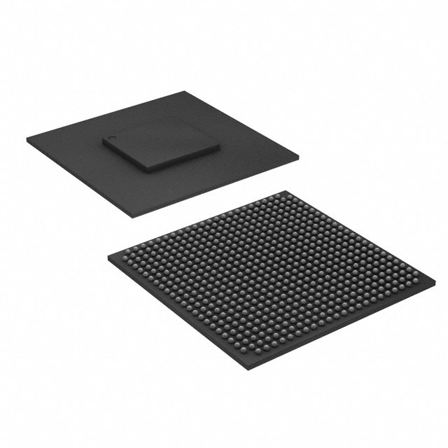
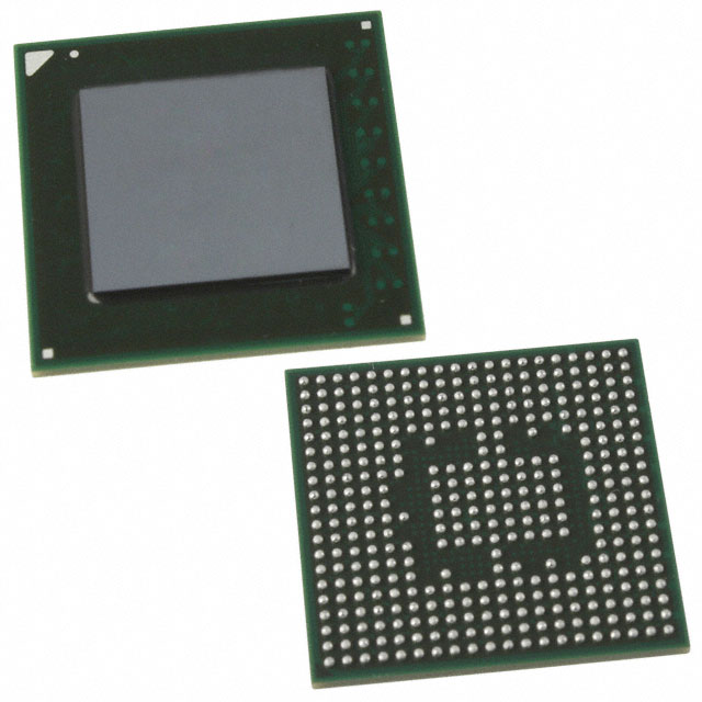
| Package / Case | 572-BGA, FCBGA | Number of I/O | 252 | Voltage | 870 mV - 930 mV | ||
| Mounting Method | Surface Mount | RoHS Compliance | RoHS Compliant | REACH Compliance | REACH Unknown | ||
| Moisture Sensitivity Level | 3 (168 Hours) | Number of LABs/CLBs | 1805 | Number of Logic Elements/Cells | 42959 | ||
| Number of Gates | N/A | ECCN | 3A991D | HTS Code | 8542.39.0001 | ||
| Qualification | N/A | Total RAM Bits | 3517440 |
Overview of EP2AGX45DF25C4N – Arria II GX Field Programmable Gate Array (FPGA) IC
The EP2AGX45DF25C4N is an Intel Arria II GX field-programmable gate array supplied in a 572-ball FCBGA package. This commercial-grade FPGA provides a balance of programmable logic capacity, embedded memory, and flexible I/O for custom digital designs and system integration.
Designed for surface-mount assembly, the device targets designs that require moderate on-chip memory, substantial logic resources, and a compact ball-grid array footprint, with specified commercial operating conditions and RoHS compliance.
Key Features
- Logic Capacity — Approximately 42,959 logic elements available for implementing custom digital functions and finite-state machines.
- Logic Array Blocks — 1,805 logic array blocks (LABs) to structure and organize logic resources within the device.
- Embedded Memory — Approximately 3.52 Mbits of on-chip RAM for buffering, FIFOs, and storage of intermediate data.
- I/O — 252 user I/Os to support diverse parallel interfaces and board-level connectivity.
- Power — Core supply specified at 870 mV to 930 mV for the device core and internal logic.
- Package & Mounting — 572-ball FCBGA (572-BGA) package, Supplier Device Package: 572-FBGA, FC (25×25); surface-mount mounting type.
- Commercial Operating Range — Rated for 0 °C to 85 °C operation, suitable for commercial temperature environments.
- Compliance — RoHS compliant for environmental and manufacturing considerations.
Typical Applications
- Custom Logic and Prototyping — Implement and iterate hardware functions, state machines, and glue logic using the device’s programmable logic resources and embedded memory.
- Data Path and Buffering — Use the on-chip memory and array of I/Os for intermediate buffering, parallel data handling, and custom data-path implementations.
- Board-Level Integration — Leverage the 252 I/Os and compact 572-ball FCBGA package for dense system designs where board real estate and connectivity matter.
Unique Advantages
- Substantial Logic Density: Approximately 42,959 logic elements enable implementation of complex combinational and sequential logic within a single device, reducing external component count.
- Organized Logic Fabric: 1,805 logic array blocks provide a structured layout for efficient resource allocation and design partitioning.
- Built‑in Memory Resources: Approximately 3.52 Mbits of embedded RAM support buffering, temporary storage, and local data handling without external memory.
- Wide I/O Footprint: 252 I/Os allow direct interfacing to parallel buses, sensors, and peripherals, simplifying board-level connectivity.
- Compact BGA Package: 572-ball FCBGA (25×25) offers a high-pin-count solution in a compact surface-mount form factor for space-constrained designs.
- Commercial Readiness: Specified for 0 °C to 85 °C operation and RoHS compliant, aligning with standard commercial manufacturing and deployment requirements.
Why Choose EP2AGX45DF25C4N?
The EP2AGX45DF25C4N positions itself as a capable commercial-grade FPGA option for designers needing significant logic resources, meaningful embedded memory, and a broad I/O complement in a compact FCBGA package. Its specified core voltage range and surface-mount packaging make it suitable for integration into mainstream embedded systems and OEM products operating within commercial temperature limits.
For teams focused on reducing BOM complexity and consolidating custom digital functions on-chip, this Arria II GX device offers a balanced mix of logic density, on-chip RAM, and connectivity—backed by RoHS compliance for mainstream manufacturing practices.
Request a quote or submit a procurement inquiry to obtain pricing, availability, and ordering information for the EP2AGX45DF25C4N.


Date Founded: 1968
Headquarters: Santa Clara, California, USA
Employees: 130,000+
Revenue: $54.23 Billion
Certifications and Memberships: ISO9001:2015, ISO14001:2015, ISO17025:2017, ISO27001:2022, ISO45001:2018, ISO50001:2018


