
EP2AGX45DF25I3G
| Part Description |
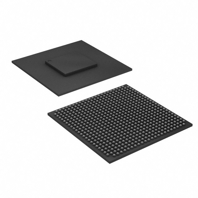
Arria II GX Field Programmable Gate Array (FPGA) IC 252 3517440 42959 572-BGA, FCBGA |
|---|---|
| Quantity | 553 Available (as of October 7, 2026) |

| Product Category | Field Programmable Gate Array (FPGA) |
|---|---|
| Manufacturer | Intel |
| Manufacturing Status | Active |
| Manufacturer Standard Lead Time | 26 Weeks |
| Datasheet |
Specifications & Environmental
| Device Package | 572-FBGA, FC (25x25) | Grade | Industrial | Operating Temperature | -40°C – 100°C | ||
|---|---|---|---|---|---|---|---|
| Package / Case | 572-BGA, FCBGA | Number of I/O | 252 | Voltage | 870 mV - 930 mV | ||
| Mounting Method | Surface Mount | RoHS Compliance | RoHS Compliant | REACH Compliance | REACH Unaffected | ||
| Moisture Sensitivity Level | 3 (168 Hours) | Number of LABs/CLBs | 1805 | Number of Logic Elements/Cells | 42959 | ||
| Number of Gates | N/A | ECCN | PENDING ECCN | HTS Code | 0000.00.0000 | ||
| Qualification | N/A | Total RAM Bits | 3517440 |
Overview of EP2AGX45DF25I3G – Arria II GX FPGA, 572‑FBGA (Industrial)
The EP2AGX45DF25I3G is an Intel Arria II GX field programmable gate array (FPGA) in a 572‑FBGA surface‑mount package, offered in an industrial temperature grade. It provides a low‑power, 40‑nm programmable logic engine and streamlined transceivers and I/Os tailored for high‑bandwidth system interfaces.
Built for designs that require high‑speed serial links, programmable logic and embedded memory, this device targets applications such as networking, telecom, embedded processing and custom accelerator functions where integration and predictable electrical and thermal characteristics matter.
Key Features
- Core Architecture 40‑nm low‑power FPGA engine with adaptive logic modules (ALMs) and eight‑input fracturable LUTs for efficient logic implementation.
- Logic Capacity 42,959 logic elements to implement mid‑to‑large scale programmable logic functions.
- Embedded Memory Approximately 3.5 Mbits of total on‑chip RAM (3,517,440 bits) for FIFOs, buffers and on‑chip data storage.
- DSP and Arithmetic High‑performance DSP blocks (documented family capability) supporting a variety of multiplier configurations for signal processing tasks.
- Transceivers & High‑Speed Interfaces Family‑level transceiver support for data rates up to 6.375 Gbps and integrated PHY functionality to simplify implementation of serial protocols.
- I/O and Termination 252 user I/O pins with on‑chip series and parallel termination options and differential termination support for robust signal integrity.
- Security & Configuration Supports 256‑bit AES programming file encryption and multiple configuration options for design protection and secure provisioning.
- Power and Voltage Documented core voltage supply range of 870 mV to 930 mV, enabling predictable power budgeting and supply design.
- Package & Mounting 572‑BGA (572‑FBGA, FC (25×25)) surface‑mount package for system integration in space‑constrained boards.
- Temperature & Reliability Industrial operating range from −40 °C to 100 °C and RoHS compliant.
Typical Applications
- Networking & Telecom Implements high‑speed serial interfaces, protocol PHYs and packet processing functions using the integrated transceivers and on‑chip memory.
- Storage & PCIe Systems Supports physical interfaces and protocol layers commonly used for PCIe and storage front‑end processing with the device family’s hard IP and I/O resources.
- Video, Imaging & Broadcast DSP blocks and embedded RAM enable buffering, filtering and real‑time signal processing for SD/HD/3G video pipelines and SDI interfaces.
- Embedded Acceleration & Custom SoC Programmable fabric and DSP resources allow implementation of custom accelerators, protocol bridging and application‑specific compute engines.
Unique Advantages
- Integrated high‑speed serial capability: Family‑level transceivers operating up to 6.375 Gbps reduce external PHY requirements for serial links and common protocols.
- Substantial logic and memory resources: 42,959 logic elements and approximately 3.5 Mbits of embedded RAM provide on‑chip capacity for control, buffering and data‑path functions.
- Industrial temperature range: Rated from −40 °C to 100 °C for deployment in temperature‑sensitive industrial applications.
- Predictable power envelope: Documented core supply range of 870–930 mV supports disciplined power design and supply selection.
- Design flow and IP support: Supported by the Quartus II and SOPC Builder toolchain and a library of hard and soft IP, facilitating integration of common interfaces and protocol blocks.
- Secure configuration options: 256‑bit AES programming file encryption for improved design confidentiality during deployment.
Why Choose EP2AGX45DF25I3G?
The EP2AGX45DF25I3G positions itself as a versatile mid‑density Arria II GX FPGA option for designs that require a combination of significant logic capacity, on‑chip memory and high‑speed serial connectivity in an industrial‑grade package. Its documented voltage and temperature ranges, together with integrated termination and configuration security, make it appropriate for systems that demand predictable electrical behavior and deployment across a wide operating environment.
Engineers can leverage the device family’s toolchain and IP ecosystem to accelerate development of networking, storage, video and embedded acceleration designs while keeping board‑level integration straightforward via the 572‑FBGA surface‑mount package and available I/O resources.
Request a quote or submit an inquiry to receive pricing and availability for the EP2AGX45DF25I3G.
























Date Founded: 1968
Headquarters: Santa Clara, California, USA
Employees: 130,000+
Revenue: $54.23 Billion
Certifications and Memberships: ISO9001:2015, ISO14001:2015, ISO17025:2017, ISO27001:2022, ISO45001:2018, ISO50001:2018


