
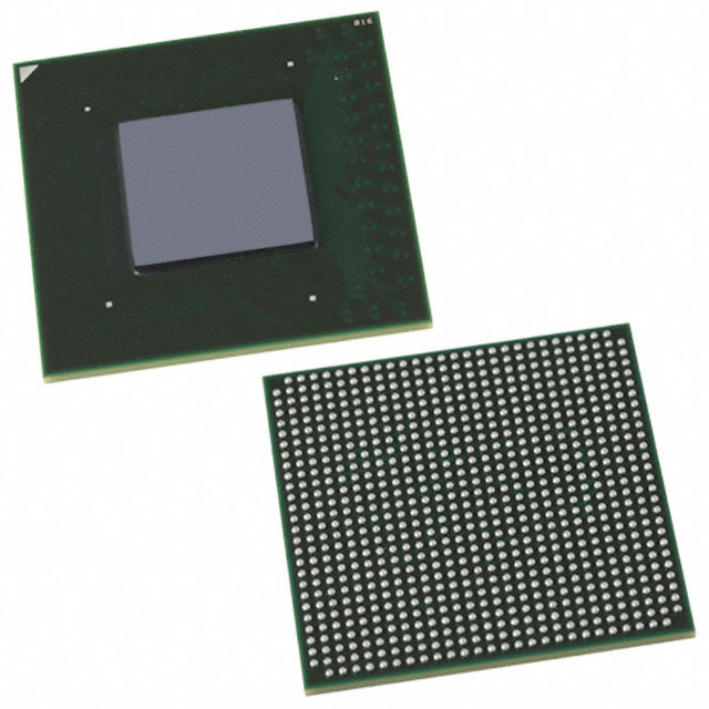
EP2AGX65DF29C5G
| Part Description |
Arria II GX Field Programmable Gate Array (FPGA) IC 364 5371904 60214 780-BBGA, FCBGA |
|---|---|
| Quantity | 1,136 Available (as of October 8, 2026) |

| Product Category | Field Programmable Gate Array (FPGA) |
|---|---|
| Manufacturer | Intel |
| Manufacturing Status | Active |
| Manufacturer Standard Lead Time | 26 Weeks |
| Datasheet |
Specifications & Environmental
| Device Package | 780-FBGA (29x29) | Grade | Commercial | Operating Temperature | 0°C – 85°C | ||
|---|---|---|---|---|---|---|---|
| Package / Case | 780-BBGA, FCBGA | Number of I/O | 364 | Voltage | 870 mV - 930 mV | ||
| Mounting Method | Surface Mount | RoHS Compliance | RoHS Compliant | REACH Compliance | REACH Unaffected | ||
| Moisture Sensitivity Level | 3 (168 Hours) | Number of LABs/CLBs | 2530 | Number of Logic Elements/Cells | 60214 | ||
| Number of Gates | N/A | ECCN | 3A991D | HTS Code | 8542.39.0001 | ||
| Qualification | N/A | Total RAM Bits | 5371904 |
Overview of EP2AGX65DF29C5G – Arria II GX FPGA, 780-BBGA (FCBGA), Commercial
The EP2AGX65DF29C5G is an Arria II GX field programmable gate array (FPGA) IC from Intel, built on a 40‑nm low‑power FPGA engine. It combines a large logic fabric with embedded memory and DSP resources to address designs that require programmable logic, signal processing, and high‑bandwidth serial interfaces.
Key device-level attributes include 60,214 logic elements, approximately 5.37 Mbits of embedded memory, 364 user I/Os, and a 780‑FBGA (29×29) surface‑mount package. The device operates from a supply range of 870 mV to 930 mV and is graded for commercial use with an operating temperature range of 0 °C to 85 °C.
Key Features
- Core & Logic 40‑nm low‑power FPGA engine with 60,214 logic elements for implementing complex, programmable logic functions.
- Embedded Memory Approximately 5.37 Mbits of on‑chip RAM for buffering, FIFOs, and local storage.
- DSP and Arithmetic Family features high‑performance DSP blocks (documented up to 550 MHz) and configurable multipliers and accumulators for signal processing tasks.
- High‑speed Transceivers & Protocol Support Arria II GX family support includes CDR‑based transceivers up to 6.375 Gbps and physical‑layer circuitry for standards such as PCIe Gen1/Gen2, Ethernet, Serial RapidIO, CPRI, and others.
- I/O and Packaging 364 user I/O pins in a 780‑FBGA (29×29) FCBGA package; surface‑mount mounting for board‑level integration.
- Power and Thermal Nominal core supply range from 870 mV to 930 mV; specified commercial operating temperature from 0 °C to 85 °C.
- Security and Configuration Device family supports 256‑bit AES programming file encryption and multiple configuration options for design security and integration.
- Design Ecosystem Family documentation highlights integrated design flows and IP support for common interfaces and memory subsystems to accelerate development.
Typical Applications
- High‑speed Communications & Networking Implements physical‑layer interfaces and protocol logic for Ethernet, PCIe, Serial RapidIO, and other serial links using integrated transceiver support.
- Data Acquisition & Signal Processing Leverages DSP blocks and embedded memory for real‑time filtering, aggregation, and preprocessing in instrumentation and test systems.
- Storage & Interconnect Useful for protocol bridging, SATA/Serial Attached SCSI, and storage controller front‑ends where programmable logic and SERDES are required.
- Broadcast and Video Transport Supports SD/HD/3G/ASI Serial Digital Interface (SDI) and related high‑bandwidth serial links for video distribution and processing.
Unique Advantages
- Significant Logic Capacity: 60,214 logic elements provide substantial programmable fabric for complex control and signal processing functions.
- Meaningful On‑Chip Memory: Approximately 5.37 Mbits of embedded RAM reduces external memory needs for many buffering and FIFO requirements.
- Comprehensive Interface Support: Family features and transceiver capabilities enable implementation of a wide range of high‑speed serial protocols and PHY functions.
- Compact, Surface‑Mount Packaging: 780‑FBGA (29×29) FCBGA package simplifies board integration while supporting a high I/O count (364 pins).
- Secure Configuration Options: 256‑bit AES programming file encryption helps protect intellectual property during device programming.
- Commercial Grade for Standard Applications: Specified operating range of 0 °C to 85 °C and defined supply range support conventional embedded and communications products.
Why Choose EP2AGX65DF29C5G?
The EP2AGX65DF29C5G positions itself as a capable programmable logic device for designs that need a balance of logic density, embedded memory, DSP capability, and high‑speed serial interface support. Its Arria II GX family heritage brings documented transceiver and PHY support alongside an established design ecosystem to shorten development time for communications, signal processing, and interface‑intensive applications.
This device is well suited to engineering teams building commercial‑grade systems that require flexible on‑chip resources, hardware security options, and a surface‑mount 780‑FBGA package with 364 I/Os. Its electrical and thermal specifications make it appropriate for standard embedded and communications product environments where the documented voltage and temperature ranges are met.
Request a quote or submit a pricing inquiry for EP2AGX65DF29C5G to obtain availability and volume pricing information tailored to your project needs.

























Date Founded: 1968
Headquarters: Santa Clara, California, USA
Employees: 130,000+
Revenue: $54.23 Billion
Certifications and Memberships: ISO9001:2015, ISO14001:2015, ISO17025:2017, ISO27001:2022, ISO45001:2018, ISO50001:2018


