
EP2AGX65DF29C6
| Part Description |
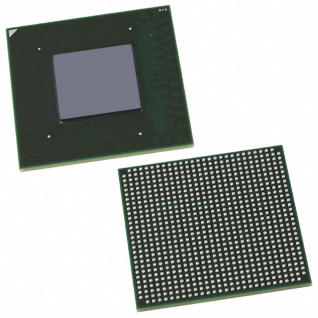
Arria II GX Field Programmable Gate Array (FPGA) IC 364 5371904 60214 780-BBGA, FCBGA |
|---|---|
| Quantity | 383 Available (as of June 15, 2026) |

| Product Category | Field Programmable Gate Array (FPGA) |
|---|---|
| Manufacturer | Intel |
| Manufacturing Status | Obsolete |
| Manufacturer Standard Lead Time | Contact Us |
| Datasheet |
Specifications & Environmental
| Device Package | 780-FBGA (29x29) | Grade | Commercial | Operating Temperature | 0°C – 85°C | ||
|---|---|---|---|---|---|---|---|
| Package / Case | 780-BBGA, FCBGA | Number of I/O | 364 | Voltage | 870 mV - 930 mV | ||
| Mounting Method | Surface Mount | RoHS Compliance | RoHS non-compliant | REACH Compliance | REACH Unknown | ||
| Moisture Sensitivity Level | 3 (168 Hours) | Number of LABs/CLBs | 2530 | Number of Logic Elements/Cells | 60214 | ||
| Number of Gates | N/A | ECCN | 3A991D | HTS Code | 8542.39.0001 | ||
| Qualification | N/A | Total RAM Bits | 5371904 |
Overview of EP2AGX65DF29C6 – Arria II GX FPGA, 780-BBGA (29×29), Surface Mount
The EP2AGX65DF29C6 is an Intel Arria II GX field programmable gate array (FPGA) supplied in a 780-ball FCBGA package and designed for commercial-grade applications. It provides a balance of logic density, embedded memory, and I/O capability suitable for mid-range FPGA implementations that require surface-mount packaging and a compact 29×29 ball footprint.
As a member of the Arria II GX family, this device benefits from the series’ documented electrical and switching characteristics, and is intended for designs that require substantial on-chip logic and memory resources within a commercial operating range.
Key Features
- Core Logic — 60,214 logic elements delivering substantial programmable logic capacity for complex combinational and sequential designs.
- Logic Array Blocks — 2,530 logic array blocks (LABs) to organize and optimize logic placement and routing.
- Embedded Memory — Approximately 5.37 Mbits of total on-chip RAM for buffering, FIFOs, and distributed storage.
- I/O Capacity — 364 user I/O pins to support multiple interfaces and board-level connectivity.
- Package & Mounting — 780-ball FCBGA (29×29) package, surface-mount mounting type, enabling high-density board integration.
- Power — Core supply range specified from 870 mV to 930 mV to match required FPGA core voltage rails.
- Commercial Temperature Grade — Rated for operation from 0 °C to 85 °C, suitable for standard commercial environments.
- Regulatory — RoHS compliant for adherence to current lead-free and restricted substances requirements.
Typical Applications
- Mid-range FPGA designs — With over 60k logic elements and several megabits of embedded RAM, the device supports complex logic integration and moderate memory requirements common to mid-range programmable designs.
- High-density I/O subsystems — 364 user I/Os provide flexibility for multi-channel interface routing, expansion headers, and board-level connectivity in communications and instrumentation products.
- Compact, board-level integration — The 780-ball FCBGA (29×29) surface-mount package enables a compact footprint for space-constrained systems where high logic density is required.
Unique Advantages
- Substantial programmable logic: 60,214 logic elements allow integration of complex state machines, custom datapaths, and control logic without external ASICs.
- Significant embedded memory: Approximately 5.37 Mbits of on-chip RAM reduces dependence on external memory for buffering and intermediate data storage.
- High I/O count: 364 I/Os enable broad interfacing options and routing flexibility for multi-protocol designs.
- Industry-standard package: 780-FBGA (29×29) package provides a known assembly footprint for high-density PCB designs.
- Commercial temperature rating: 0 °C to 85 °C supports a wide range of commercial applications and environments.
- Regulatory compliance: RoHS compliance simplifies design for markets requiring restricted-substance adherence.
Why Choose EP2AGX65DF29C6?
The EP2AGX65DF29C6 positions itself as a commercially rated Arria II GX FPGA that combines a large logic element count with multiple megabits of embedded RAM and a high I/O complement in a 780-ball FCBGA package. Its core voltage range and commercial temperature spec make it suitable for mainstream embedded and board-level applications that demand compact packaging and considerable programmable resources.
This device is an appropriate choice for engineering teams seeking to consolidate logic, memory, and I/O on a single programmable device while maintaining compliance with RoHS requirements and using a standardized package for high-density PCB assembly.
Request a quote or submit an inquiry to get pricing and availability for EP2AGX65DF29C6 and to discuss how it fits your next FPGA design.


Date Founded: 1968
Headquarters: Santa Clara, California, USA
Employees: 130,000+
Revenue: $54.23 Billion
Certifications and Memberships: ISO9001:2015, ISO14001:2015, ISO17025:2017, ISO27001:2022, ISO45001:2018, ISO50001:2018


