
EP2AGX65DF29C6G
| Part Description |
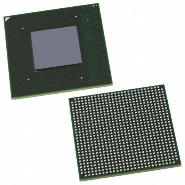
Arria II GX Field Programmable Gate Array (FPGA) IC 364 5371904 60214 780-BBGA, FCBGA |
|---|---|
| Quantity | 251 Available (as of June 15, 2026) |

| Product Category | Field Programmable Gate Array (FPGA) |
|---|---|
| Manufacturer | Intel |
| Manufacturing Status | Active |
| Manufacturer Standard Lead Time | 26 Weeks |
| Datasheet |
Specifications & Environmental
| Device Package | 780-FBGA (29x29) | Grade | Commercial | Operating Temperature | 0°C – 85°C | ||
|---|---|---|---|---|---|---|---|
| Package / Case | 780-BBGA, FCBGA | Number of I/O | 364 | Voltage | 870 mV - 930 mV | ||
| Mounting Method | Surface Mount | RoHS Compliance | RoHS Compliant | REACH Compliance | REACH Unaffected | ||
| Moisture Sensitivity Level | 3 (168 Hours) | Number of LABs/CLBs | 2530 | Number of Logic Elements/Cells | 60214 | ||
| Number of Gates | N/A | ECCN | 3A991D | HTS Code | 8542.39.0001 | ||
| Qualification | N/A | Total RAM Bits | 5371904 |
Overview of EP2AGX65DF29C6G – Arria II GX FPGA, 60,214 Logic Elements, 364 I/Os, 780-BBGA (29×29)
The EP2AGX65DF29C6G is an Intel Arria II GX field-programmable gate array (FPGA) supplied in a 780-BBGA FCBGA package. It combines a 40‑nm low-power FPGA engine and Arria II family architecture features to support designs that require programmable logic, embedded memory and high‑speed serial and parallel I/O.
With 60,214 logic elements, approximately 5.37 Mbits of embedded memory, and 364 I/Os, this commercial‑grade device is suitable for applications needing mid-range programmable logic density, integrated DSP and transceiver-capable interfaces within a surface‑mount 29×29 mm package.
Key Features
- Logic Capacity — 60,214 logic elements suitable for mid-range FPGA designs, built on the Arria II device architecture.
- Embedded Memory — Approximately 5.37 Mbits of on‑chip RAM for FIFOs, buffering and intermediate storage.
- I/O Density — 364 user I/Os to support a mix of parallel and serial interfaces in multi‑bank configurations.
- Transceivers and Protocol Support — Arria II family features include transceivers and dedicated physical‑layer circuitry that support common serial protocols and high‑bandwidth interfaces (as described in the Arria II device handbook).
- DSP and Arithmetic Resources — Family-level DSP blocks and multiplier/add accumulation features are available for signal processing and arithmetic acceleration (see Arria II documentation for device-level details).
- Package and Mounting — 780-BBGA, FCBGA (supplier package: 780‑FBGA, 29×29 mm) designed for surface-mount assembly.
- Power and Voltage — Nominal supply range specified at 870 mV to 930 mV.
- Operating Range — Commercial operating temperature from 0 °C to 85 °C; RoHS compliant.
Typical Applications
- Networking and Communications — Implement protocol handling, serialization/deserialization and data buffering using the device’s embedded memory, DSP capabilities and Arria II transceiver features.
- Imaging and Signal Processing — Use on‑chip DSP resources and logic elements for intermediate image processing, filtering and real‑time data manipulation.
- Prototyping and Embedded Systems — Mid-density programmable fabric and abundant I/O make this device suitable for system prototypes and embedded control platforms requiring customizable logic and memory.
- Storage and Interface Bridging — Employ embedded memory and I/O mix to implement interface bridging, buffering and protocol adaptation in storage or peripheral subsystems.
Unique Advantages
- Balanced Logic and Memory — 60,214 logic elements paired with approximately 5.37 Mbits of embedded RAM provide a practical balance for designs needing both compute and buffering on a single device.
- High I/O Count — 364 user I/Os facilitate dense interfacing with external peripherals, memory interfaces and parallel buses, reducing external glue logic.
- Arria II Family Capabilities — Device benefits from Arria II architectural features documented in the device handbook, including DSP resources and transceiver support for common serial protocols.
- Compact Surface‑Mount Package — 780‑BBGA (29×29) package supports high pin count in a compact footprint suitable for board-level integration.
- Commercial Temperature and RoHS Compliance — Rated for 0 °C to 85 °C operation and RoHS compliant for mainstream commercial applications.
Why Choose EP2AGX65DF29C6G?
The EP2AGX65DF29C6G delivers a combination of mid-range logic density, substantial embedded memory and a high I/O count within a surface-mount 780‑BBGA package. It is positioned for designers who need programmable logic with integrated memory and Arria II family features for communications, signal processing and embedded system applications.
Backed by the Arria II device documentation and Intel’s FPGA ecosystem, this device provides a scalable, documented platform for development and deployment where commercial temperature operation and RoHS compliance are required.
Request a quote or submit a procurement inquiry today to receive pricing and availability for the EP2AGX65DF29C6G.


Date Founded: 1968
Headquarters: Santa Clara, California, USA
Employees: 130,000+
Revenue: $54.23 Billion
Certifications and Memberships: ISO9001:2015, ISO14001:2015, ISO17025:2017, ISO27001:2022, ISO45001:2018, ISO50001:2018


