
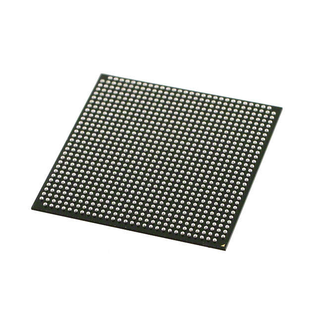
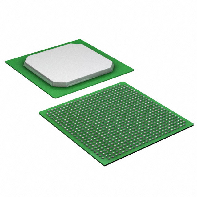
EP2C70F896C7N
| Part Description |
Cyclone® II Field Programmable Gate Array (FPGA) IC 622 1152000 68416 896-BGA |
|---|---|
| Quantity | 66 Available (as of June 15, 2026) |
| Product Category | Field Programmable Gate Array (FPGA) |
|---|---|
| Manufacturer | Intel |
| Manufacturing Status | Active |
| Manufacturer Standard Lead Time | 26 Weeks |
| Datasheet |
Specifications & Environmental
| Device Package | 896-FBGA (31x31) | Grade | Commercial | Operating Temperature | 0°C – 85°C | ||
|---|---|---|---|---|---|---|---|
| Package / Case | 896-BGA | Number of I/O | 622 | Voltage | 1.15 V - 1.25 V | ||
| Mounting Method | Surface Mount | RoHS Compliance | RoHS Compliant | REACH Compliance | REACH Unaffected | ||
| Moisture Sensitivity Level | 3 (168 Hours) | Number of LABs/CLBs | 4276 | Number of Logic Elements/Cells | 68416 | ||
| Number of Gates | N/A | ECCN | 3A001A7A | HTS Code | 8542.39.0001 | ||
| Qualification | N/A | Total RAM Bits | 1152000 |
Overview of EP2C70F896C7N – Cyclone® II FPGA, 68,416 logic elements, ≈1.15 Mbits RAM, 896-BGA
The EP2C70F896C7N is a Cyclone® II field programmable gate array (FPGA) offered in a 896-ball BGA package for surface-mount assembly. It delivers a combination of high logic density, substantial on-chip memory, and a large I/O count suited to commercial embedded processing and DSP-focused designs.
Designed as part of the Cyclone II family, the device is documented in the Cyclone II Device Handbook and includes architecture-level features such as embedded memory, multipliers, and clocking resources to support configurable logic implementations in commercial electronic systems.
Key Features
- Core Logic 68,416 logic elements provide significant configurable logic capacity for complex glue logic, protocol bridging, and custom datapaths.
- Embedded Memory Approximately 1.15 Mbits of on-chip RAM to support buffers, FIFOs, and local data storage for processing tasks.
- I/O Resources 622 user I/O pins enable broad connectivity for parallel buses, external memory interfaces, and mixed-signal front-ends.
- Clocking and Timing Family documentation details a global clock network and phase-locked loops (PLLs) to support flexible clock distribution and frequency synthesis.
- DSP Support The device family includes embedded multipliers and dedicated routing for arithmetic-intensive operations commonly used in DSP applications.
- Package & Mounting 896-FBGA (31×31 mm) package, surface-mount mounting type, suitable for compact board-level integration.
- Power and Operating Range Core supply voltage range 1.15 V to 1.25 V with an ambient operating temperature range of 0 °C to 85 °C (commercial grade).
- Compliance RoHS compliant.
Typical Applications
- Low-cost embedded processing — Implements custom control, protocol handling, and finite-state machines for commercial electronics as identified in Cyclone II documentation.
- DSP and signal processing — Uses embedded multipliers and on-chip RAM for algorithm acceleration and data buffering in real-time processing tasks.
- Memory interface bridging — Provides the logic and I/O resources needed for interfacing with external memory and peripherals.
- High-density I/O control — Supports systems requiring many parallel or multi-standard I/O connections such as display controllers, sensor arrays, or communication front-ends.
Unique Advantages
- High logic density: 68,416 logic elements allow consolidation of multiple functions into a single device, reducing BOM and board area.
- Substantial embedded memory: Approximately 1.15 Mbits of on-chip RAM minimizes external memory dependence for many buffering and storage needs.
- Extensive I/O: 622 I/O pins provide design flexibility for large bus interfaces and mixed-signal connectivity.
- Flexible clocking: Integrated PLLs and global clock network support multiple clock domains and precise timing management.
- Commercial-grade, RoHS compliant: Suitable for commercial electronic product lifecycles with environmental compliance.
- Compact package: 896-FBGA (31×31) delivers dense integration for space-constrained PCB designs.
Why Choose EP2C70F896C7N?
The EP2C70F896C7N positions itself as a high-capacity Cyclone II FPGA option for commercial embedded and DSP applications that require large logic resources, ample on-chip memory, and extensive I/O. Its documented architecture—covering logic array blocks, embedded multipliers, memory modes, and clocking resources—supports flexible implementation of custom digital functions.
Backed by the Cyclone II Device Handbook and family-level documentation, this device is suitable for design teams seeking a commercially graded FPGA platform with verified architectural features, established design references, and the integration density needed to reduce system complexity.
Request a quote or submit an inquiry to evaluate EP2C70F896C7N for your next commercial FPGA design project.


Date Founded: 1968
Headquarters: Santa Clara, California, USA
Employees: 130,000+
Revenue: $54.23 Billion
Certifications and Memberships: ISO9001:2015, ISO14001:2015, ISO17025:2017, ISO27001:2022, ISO45001:2018, ISO50001:2018


