
EP2C8F256C6N
| Part Description |
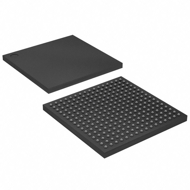
Cyclone® II Field Programmable Gate Array (FPGA) IC 182 165888 8256 256-LBGA |
|---|---|
| Quantity | 1,579 Available (as of October 7, 2026) |

| Product Category | Field Programmable Gate Array (FPGA) |
|---|---|
| Manufacturer | Intel |
| Manufacturing Status | Active |
| Manufacturer Standard Lead Time | 26 Weeks |
| Datasheet |
Specifications & Environmental
| Device Package | 256-FBGA (17x17) | Grade | Commercial | Operating Temperature | 0°C – 85°C | ||
|---|---|---|---|---|---|---|---|
| Package / Case | 256-LBGA | Number of I/O | 182 | Voltage | 1.15 V - 1.25 V | ||
| Mounting Method | Surface Mount | RoHS Compliance | RoHS Compliant | REACH Compliance | REACH Unaffected | ||
| Moisture Sensitivity Level | 3 (168 Hours) | Number of LABs/CLBs | 516 | Number of Logic Elements/Cells | 8256 | ||
| Number of Gates | N/A | ECCN | 3A991D | HTS Code | 8542.39.0001 | ||
| Qualification | N/A | Total RAM Bits | 165888 |
Overview of EP2C8F256C6N – Cyclone® II Field Programmable Gate Array (FPGA), 8,256 logic elements, 256‑LBGA
The EP2C8F256C6N is a Cyclone® II family FPGA from Intel, combining 8,256 logic elements and family-level architecture features tailored for low-cost embedded processing and DSP-oriented designs. Its on‑chip resources and I/O complement make it suitable for medium-density logic integration, memory‑rich functions, and multi‑interface subsystems in commercial applications.
As a member of the Cyclone II device family, this device leverages documented architecture elements such as embedded memory blocks, programmable clock resources, and flexible I/O capabilities to simplify system integration while operating within a commercial temperature range.
Key Features
- Logic Capacity 8,256 logic elements distributed across 516 LABs, providing medium-density programmable logic for control, glue logic, and embedded processing functions.
- Embedded Memory Approximately 0.166 Mbits of on‑chip RAM (165,888 total RAM bits) for local buffering, FIFOs, and small embedded datasets.
- I/O Resources 182 user I/O pins to support multiple parallel interfaces and peripheral connections.
- Power Supply Core voltage range of 1.15 V to 1.25 V, enabling compatibility with Cyclone II family power architectures.
- Package & Mounting 256‑ball LBGA package (supplier device package: 256‑FBGA, 17 × 17 mm) designed for surface‑mount assembly in compact system boards.
- Operating Grade Commercial grade operation from 0 °C to 85 °C, suitable for a wide range of consumer and commercial applications.
- Cyclone II Family Architecture Family features documented in the Cyclone II Device Handbook include global clock networks and phase‑locked loops (PLLs), embedded M4K memory blocks, embedded multipliers, and flexible I/O structure and standards.
- Regulatory Compliance RoHS compliant for compatibility with modern manufacturing and environmental requirements.
Typical Applications
- Embedded Processing Implement soft processors, control logic, and protocol bridging using the device’s logic elements and on‑chip memory.
- DSP and Signal Conditioning Leverage Cyclone II family DSP features and embedded multipliers for medium‑complexity signal processing tasks and filtering.
- Interface and Peripheral Control Use the 182 I/Os for parallel/serial peripheral interfaces, sensor aggregation, and control of external memory or devices.
- Low‑Cost FPGA Integration Ideal for designs that require cost‑efficient programmable logic with documented family resources such as clock networks, configuration options, and embedded memory.
Unique Advantages
- Moderate Logic Density: 8,256 logic elements provide a balance between capacity and cost for medium‑complexity designs.
- Embedded Memory Onboard: 165,888 bits of RAM reduce external memory needs for buffering and small data storage, simplifying board design.
- Flexible I/O Count: 182 I/Os enable multiple peripheral connections without immediate need for expanders, lowering BOM and PCB complexity.
- Compact Surface‑Mount Package: 256‑LBGA (17 × 17 mm supplier FBGA) offers a compact footprint for space‑constrained applications.
- Commercial Temperature Range: Rated 0 °C to 85 °C to match consumer and commercial product operating environments.
- Documented Family Support: Backed by the Cyclone II Device Handbook and Cyclone II family documentation for architecture, configuration, and timing guidance.
Why Choose EP2C8F256C6N?
The EP2C8F256C6N positions itself as a cost‑effective Cyclone II FPGA option for engineers needing a medium‑density programmable device with on‑chip memory and a generous I/O complement. Its combination of 8,256 logic elements, approximately 0.166 Mbits of embedded RAM, and 182 I/Os helps simplify integration of control, interface, and moderate DSP tasks within commercial product designs.
With a compact 256‑LBGA surface‑mount package, RoHS compliance, and support materials in the Cyclone II device handbook, this device is suited for development teams focused on predictable integration, documented design flows, and commercial‑grade deployments.
Request a quote or submit an inquiry to receive pricing, availability, and ordering information for EP2C8F256C6N. Our team can provide lead time details and support for your evaluation and production planning needs.























Date Founded: 1968
Headquarters: Santa Clara, California, USA
Employees: 130,000+
Revenue: $54.23 Billion
Certifications and Memberships: ISO9001:2015, ISO14001:2015, ISO17025:2017, ISO27001:2022, ISO45001:2018, ISO50001:2018


