
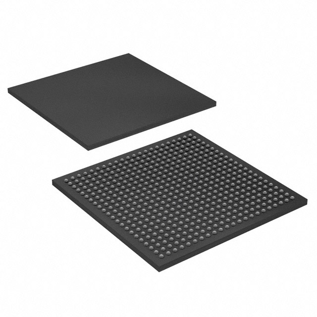
EP2S30F484C4
| Part Description |
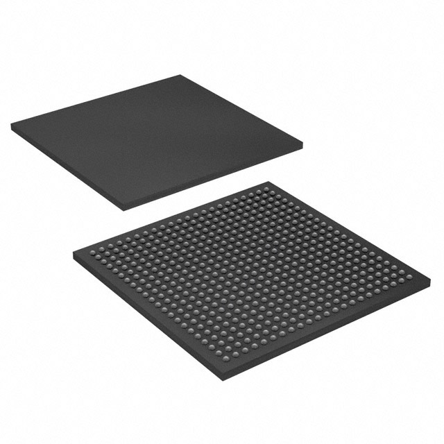
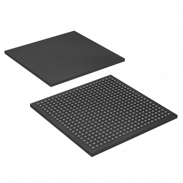
Stratix® II Field Programmable Gate Array (FPGA) IC 342 1369728 33880 484-BBGA |
|---|---|
| Quantity | 1,554 Available (as of October 7, 2026) |
| Product Category | Field Programmable Gate Array (FPGA) |
|---|---|
| Manufacturer | Intel |
| Manufacturing Status | Obsolete |
| Manufacturer Standard Lead Time | Contact Us |
| Datasheet |
Specifications & Environmental
| Device Package | 484-FBGA (23x23) | Grade | Commercial | Operating Temperature | 0°C – 85°C | ||
|---|---|---|---|---|---|---|---|
| Package / Case | 484-BBGA | Number of I/O | 342 | Voltage | 1.15 V - 1.25 V | ||
| Mounting Method | Surface Mount | RoHS Compliance | RoHS non-compliant | REACH Compliance | REACH Unaffected | ||
| Moisture Sensitivity Level | 3 (168 Hours) | Number of LABs/CLBs | 1694 | Number of Logic Elements/Cells | 33880 | ||
| Number of Gates | N/A | ECCN | 3A991D | HTS Code | 8542.39.0001 | ||
| Qualification | N/A | Total RAM Bits | 1369728 |
Overview of EP2S30F484C4 – Stratix® II FPGA, 33,880 Logic Elements, 342 I/O, 484‑BBGA
The EP2S30F484C4 is a Stratix II field-programmable gate array (FPGA) IC from Intel (Stratix II device family) designed for complex digital designs that require substantial logic capacity, on‑chip memory, and flexible I/O. Its architecture includes dedicated DSP resources, programmable clock networks and PLLs, and a multi‑track interconnect fabric documented in the Stratix II device handbook.
This commercial‑grade, surface‑mount 484‑BBGA device is targeted at applications needing high logic density, significant embedded memory, and advanced I/O structure within a compact package footprint.
Key Features
- Core Logic Provides 33,880 logic elements for implementing large-scale custom logic and state machines.
- Logic Array Blocks (LABs) Contains 1,694 LABs (logic array blocks) to organize and optimize logic placement and routing.
- Embedded Memory Includes a total of 1,369,728 bits of on‑chip RAM — approximately 1.37 Mbits of embedded memory for buffering, FIFOs and local storage.
- I/O Capacity & Structure Equipped with 342 I/O pins; the device handbook documents advanced I/O structure, double data‑rate support and high‑speed I/O options for diverse interface needs.
- DSP & Clocking Stratix II architecture provides dedicated digital signal processing blocks plus enhanced and fast PLLs and hierarchical clock networks for precise timing and signal processing tasks.
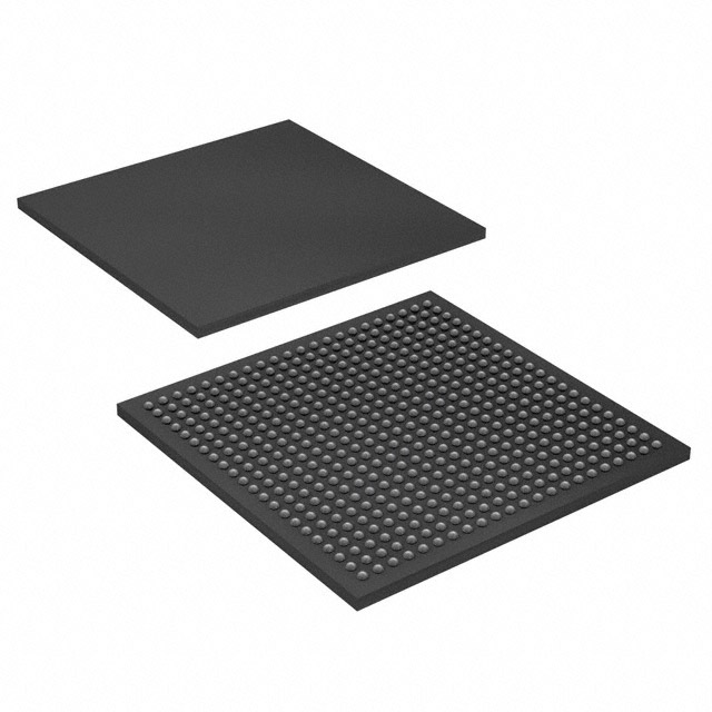
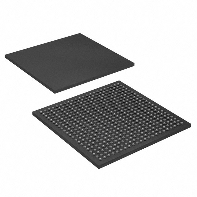
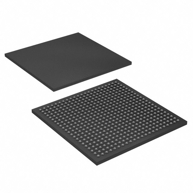
- Package & Mounting Surface mount 484‑BBGA package (484‑FBGA, 23×23) for compact board integration and reliable solder mounting.
- Power & Temperature Operational core supply range of 1.15 V to 1.25 V; commercial operating temperature range 0 °C to 85 °C.
- Compliance RoHS compliant for environmental regulatory conformity.
Typical Applications
- High‑Performance Digital Signal Processing Use the built‑in DSP blocks and embedded memory for filtering, modulation, and real‑time signal pipelines.
- Communications and Networking Deploy for packet processing, protocol bridging, and interface adaptation leveraging the device's high I/O count and clocking resources.
- Memory Interface and Controllers Implement external RAM interfacing and custom memory controllers using the device's embedded memory and documented external memory interface capabilities.
- Custom Logic and Prototyping Ideal for OEMs and system designers implementing custom accelerators, controllers, or glue logic where a programmable hardware approach is required.
Unique Advantages
- High logic density: 33,880 logic elements let you consolidate complex functions into a single FPGA, reducing board-level BOM and interconnect complexity.
- Substantial on‑chip memory: Approximately 1.37 Mbits of embedded RAM supports buffering and local storage to improve throughput and deterministic behavior.
- Robust I/O capability: 342 I/O pins and documented high‑speed I/O support enable flexible interfacing with peripherals and high‑rate links.
- Dedicated DSP and clock resources: On‑chip DSP blocks plus enhanced/fast PLLs and hierarchical clocking support deterministic signal processing and low‑jitter clock domains.
- Compact BGAs for dense layouts: The 484‑FBGA (23×23) package provides a compact form factor suitable for space‑constrained PCBs while maintaining a high pin count.
- Commercial readiness and compliance: Commercial grade device with RoHS compliance suitable for a wide range of commercial electronic products.
Why Choose EP2S30F484C4?
The EP2S30F484C4 combines substantial logic capacity, meaningful on‑chip memory, and extensive I/O in a compact 484‑BBGA package, making it a practical choice for designs that require programmable hardware acceleration, complex protocol handling, or tight integration of DSP and control logic. Its Stratix II architecture and documented features (DSP blocks, PLLs, multi‑track interconnect, and I/O structure) provide the architectural building blocks to implement performance‑oriented custom silicon functions.
Backed by the Stratix II device handbook and Intel's device documentation, EP2S30F484C4 is well suited for engineering teams and procurement groups building medium‑to‑high complexity commercial electronics who need a reliable, programmable platform with verified design guidance and on‑chip resources.
Request a quote or submit a purchase inquiry to evaluate EP2S30F484C4 for your next design project and obtain pricing and availability information.




















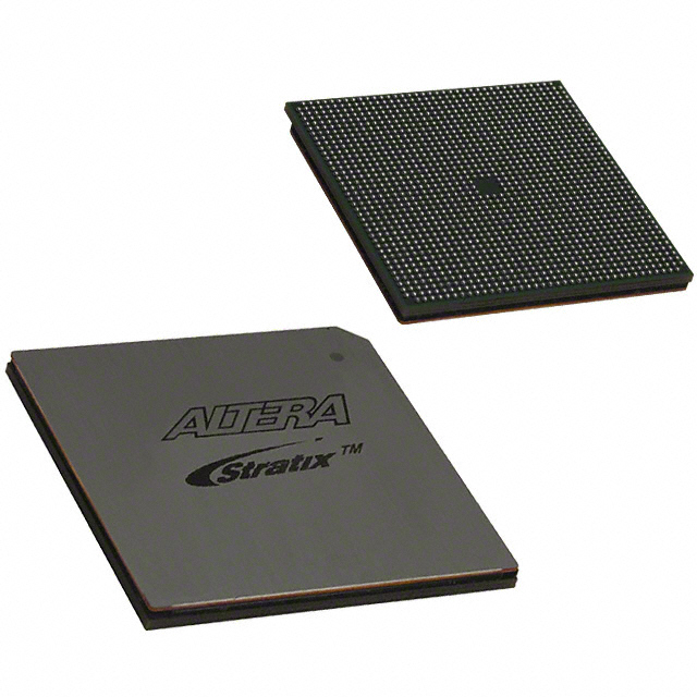
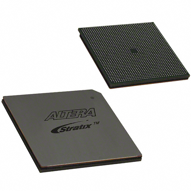
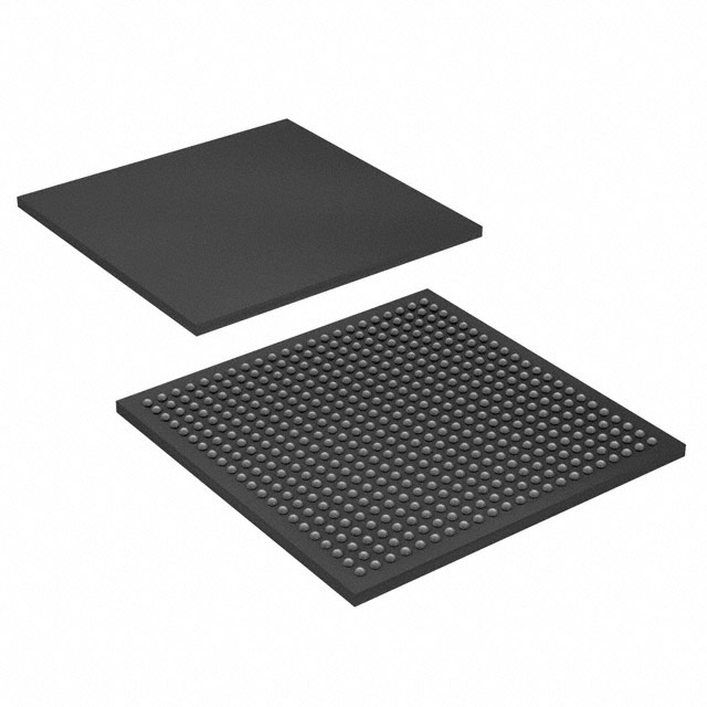

Date Founded: 1968
Headquarters: Santa Clara, California, USA
Employees: 130,000+
Revenue: $54.23 Billion
Certifications and Memberships: ISO9001:2015, ISO14001:2015, ISO17025:2017, ISO27001:2022, ISO45001:2018, ISO50001:2018


