
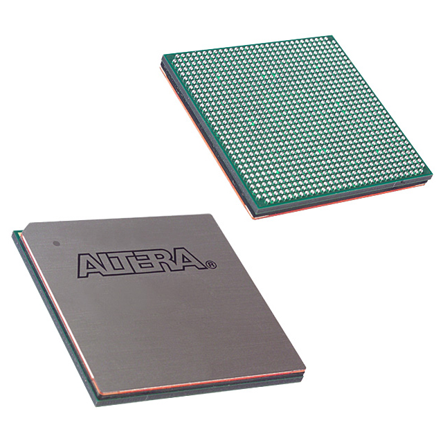
EP2S60F1020C3
| Part Description |
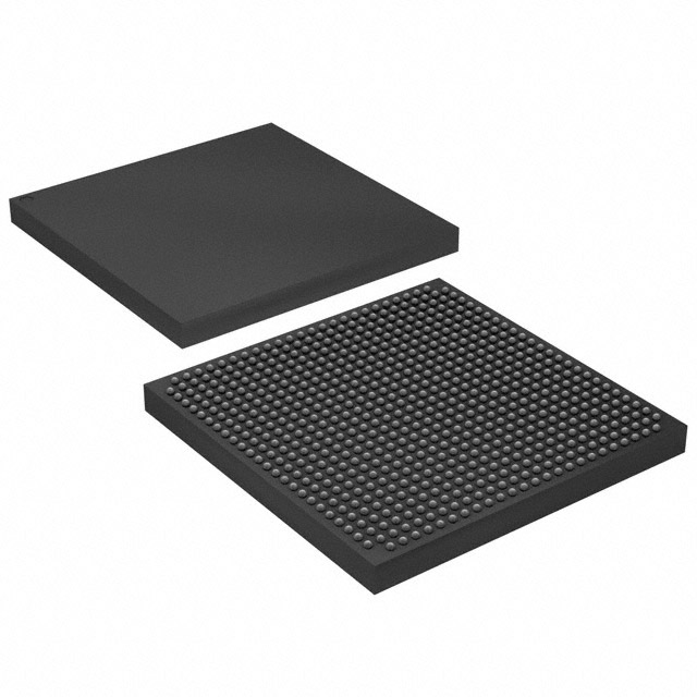
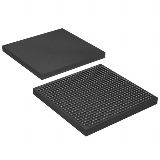
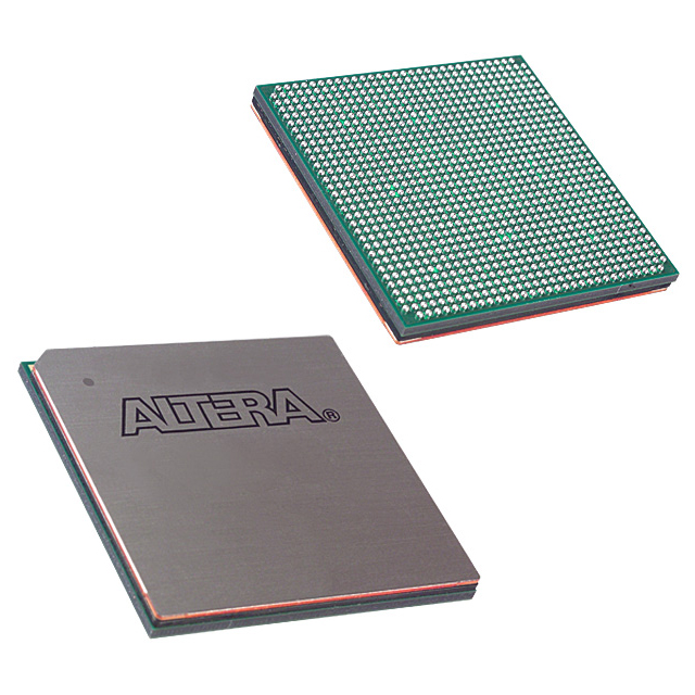
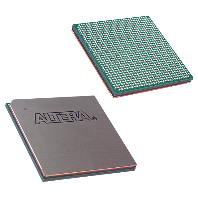
Stratix® II Field Programmable Gate Array (FPGA) IC 718 2544192 60440 1020-BBGA |
|---|---|
| Quantity | 612 Available (as of October 8, 2026) |
| Product Category | Field Programmable Gate Array (FPGA) |
|---|---|
| Manufacturer | Intel |
| Manufacturing Status | Obsolete |
| Manufacturer Standard Lead Time | Contact Us |
| Datasheet |
Specifications & Environmental
| Device Package | 1020-FBGA (33x33) | Grade | Commercial | Operating Temperature | 0°C – 85°C | ||
|---|---|---|---|---|---|---|---|
| Package / Case | 1020-BBGA | Number of I/O | 718 | Voltage | 1.15 V - 1.25 V | ||
| Mounting Method | Surface Mount | RoHS Compliance | RoHS non-compliant | REACH Compliance | REACH Unaffected | ||
| Moisture Sensitivity Level | 3 (168 Hours) | Number of LABs/CLBs | 3022 | Number of Logic Elements/Cells | 60440 | ||
| Number of Gates | N/A | ECCN | 3A001A7A | HTS Code | 8542.39.0001 | ||
| Qualification | N/A | Total RAM Bits | 2544192 |
Overview of EP2S60F1020C3 – Stratix® II Field Programmable Gate Array (FPGA) IC 718 2544192 60440 1020-BBGA
The EP2S60F1020C3 is an Intel Stratix II field programmable gate array designed for applications that require substantial programmable logic, embedded memory, and large I/O counts. As a member of the Stratix II family, the device integrates core FPGA capabilities alongside on-chip memory and clocking resources described in the device handbook.
Key hardware characteristics include 60,440 logic elements, approximately 2.54 Mbits of embedded memory, and 718 user I/O pins, making the device suitable for dense logic integration, memory‑rich designs, and systems with extensive external interfacing needs.
Key Features
- Core Logic Capacity — 60,440 logic elements to implement complex, high‑density logic functions and custom datapaths.
- Embedded Memory — Total on‑chip RAM of 2,544,192 bits (approximately 2.54 Mbits) for local buffering, FIFOs, and implemented state machines.
- I/O Resources — 718 general-purpose I/Os to support wide parallel buses and multiple external interfaces; device documentation details support for advanced I/O standards and DDR operation.
- Clocking and DSP — Stratix II architecture includes PLLs, global and hierarchical clock networks, and DSP block support as documented in the device handbook for timing and signal processing requirements.
- Configuration and Debug Support — Device family features in the handbook include IEEE 1149.1 JTAG boundary‑scan and SignalTap II embedded logic analyzer support for in-system debug and configuration.
- Power and Voltage — Core supply range specified at 1.15 V to 1.25 V for compatibility with Stratix II power architectures.
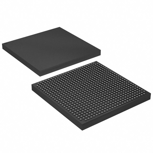
- Package and Mounting — 1020‑BBGA package (supplier device package 1020‑FBGA, 33×33) in a surface‑mount form factor for compact board-level integration.
- Commercial Grade Temperature — Rated for operation from 0 °C to 85 °C, intended for commercial‑temperature applications.
- RoHS Compliant — Meets RoHS requirements for reduced hazardous substances.
Typical Applications
- Advanced Prototyping and Emulation — Large logic capacity and on‑chip memory enable complex hardware prototypes and system emulation tasks.
- High‑density Control and Signal Processing — DSP blocks combined with abundant logic and embedded RAM support custom signal processing pipelines and real‑time control functions.
- High‑I/O Interfaces — 718 I/Os facilitate wide parallel buses, multi‑lane interfaces, and extensive peripheral connectivity on a single device.
- Complex System Integration — Compact 1020‑BBGA packaging simplifies board layout for space‑constrained systems that require significant logic and I/O resources.
Unique Advantages
- High logic density: 60,440 logic elements allow consolidation of multiple functions into a single FPGA, reducing component count and board complexity.
- Substantial on‑chip memory: Approximately 2.54 Mbits of embedded RAM provides local storage for buffering, packet processing, and state retention without external memory.
- Extensive I/O availability: 718 I/Os support diverse peripheral and bus connections, enabling flexible system partitioning.
- Integrated timing and DSP resources: On‑device PLLs, clock networks, and DSP support simplify implementation of synchronized, high‑performance datapaths.
- Compact, manufacturable package: 1020‑BBGA (1020‑FBGA, 33×33) surface‑mount packaging balances pin density with board‑level manufacturability.
- RoHS compliant and commercial grade: Meets RoHS requirements and operates across a 0 °C to 85 °C commercial temperature range for mainstream electronic products.
Why Choose EP2S60F1020C3?
The EP2S60F1020C3 positions itself as a robust Stratix II FPGA option for designers who need a combination of high logic capacity, meaningful on‑chip memory, and a large number of I/Os in a compact BGA package. Its Stratix II architecture features—documented PLLs, clocking resources, DSP blocks, and configuration/debug facilities—support complex designs that require synchronized timing and in‑system visibility.
This device is well suited for engineering teams building memory‑intensive logic, multi‑interface systems, or consolidated digital subsystems where integration, board space, and predictable commercial‑temperature operation are priorities. The device handbook and datasheet provide the detailed electrical, timing, and configuration specifications needed to design and validate systems around this FPGA.
Request a quote or submit a request for pricing and availability for EP2S60F1020C3 to obtain detailed lead‑time and procurement information.






















Date Founded: 1968
Headquarters: Santa Clara, California, USA
Employees: 130,000+
Revenue: $54.23 Billion
Certifications and Memberships: ISO9001:2015, ISO14001:2015, ISO17025:2017, ISO27001:2022, ISO45001:2018, ISO50001:2018


