
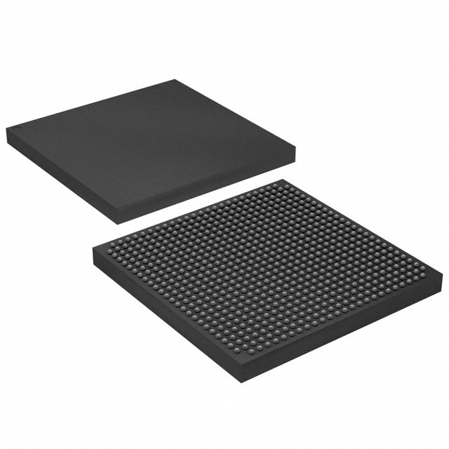
EP2S60F672C5N
| Part Description |
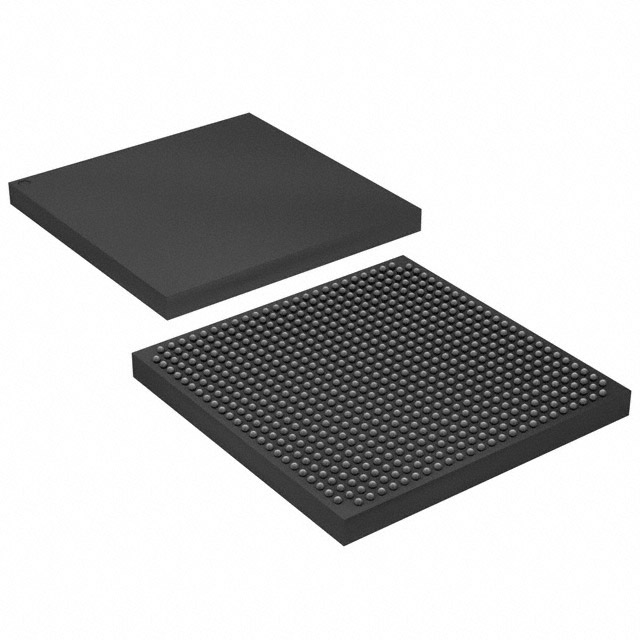
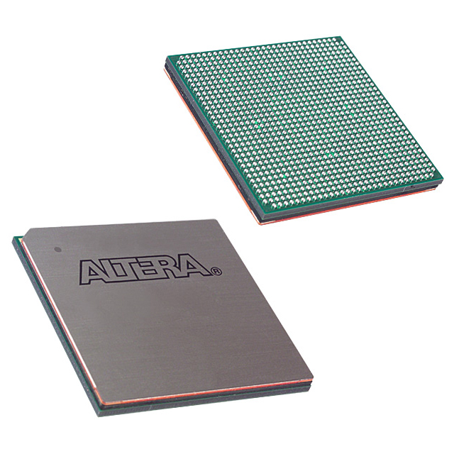
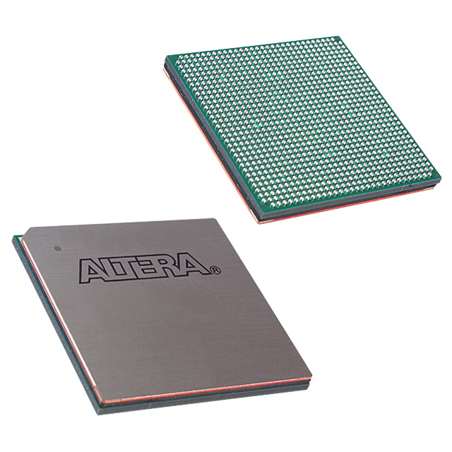
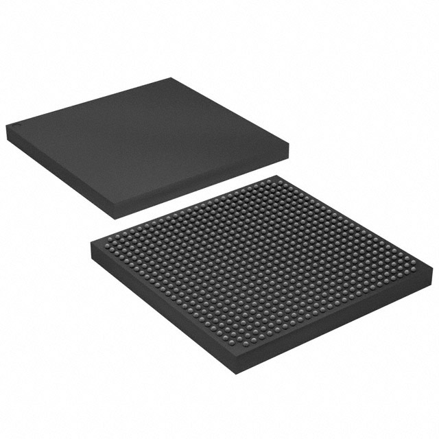
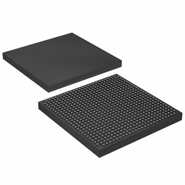
Stratix® II Field Programmable Gate Array (FPGA) IC 492 2544192 60440 672-BBGA |
|---|---|
| Quantity | 1,238 Available (as of October 7, 2026) |
| Product Category | Field Programmable Gate Array (FPGA) |
|---|---|
| Manufacturer | Intel |
| Manufacturing Status | Obsolete |
| Manufacturer Standard Lead Time | Contact Us |
| Datasheet |
Specifications & Environmental
| Device Package | 672-FBGA (27x27) | Grade | Commercial | Operating Temperature | 0°C – 85°C | ||
|---|---|---|---|---|---|---|---|
| Package / Case | 672-BBGA | Number of I/O | 492 | Voltage | 1.15 V - 1.25 V | ||
| Mounting Method | Surface Mount | RoHS Compliance | RoHS Compliant | REACH Compliance | REACH Unaffected | ||
| Moisture Sensitivity Level | 3 (168 Hours) | Number of LABs/CLBs | 3022 | Number of Logic Elements/Cells | 60440 | ||
| Number of Gates | N/A | ECCN | 3A991D | HTS Code | 8542.39.0001 | ||
| Qualification | N/A | Total RAM Bits | 2544192 |
Overview of EP2S60F672C5N – Stratix® II Field Programmable Gate Array, 672-BBGA, 1.15–1.25 V
The EP2S60F672C5N is a Stratix® II family Field Programmable Gate Array (FPGA) supplied in a 672-ball BGA package. It integrates a large programmable fabric with on-chip memory, dedicated DSP circuitry and advanced I/O infrastructure for demanding digital designs.
With 60,440 logic elements, approximately 2.54 Mbits of embedded memory and 492 I/O pins, this device targets high-density logic, memory-interface and signal-processing applications that require tight integration and flexible I/O and clocking resources.
Key Features
- Logic Capacity — 60,440 logic elements to implement complex digital functions and custom hardware accelerators.
- Embedded Memory — Approximately 2.54 Mbits of on-chip RAM for buffering, packet storage and on-chip data structures.
- I/O Resources — 492 user I/O pins supporting a wide range of external interfaces and high-pin-count connectivity.
- Package & Mounting — 672-BBGA package; supplier device package 672-FBGA (27×27 mm). Surface-mount mounting for board-level integration.
- Power Supply — Core voltage operating range from 1.15 V to 1.25 V to match system power rails.
- Commercial Temperature Grade — Rated for 0 °C to 85 °C operating temperature for standard commercial applications.
- Stratix II Family Architecture — Family-level features from the Stratix II handbook such as advanced PLLs and global clock networks to manage timing and clock distribution across the device.
- High-Speed I/O and Interface Support — Device handbook coverage includes high-speed differential I/O, programmable drive strengths, on‑chip termination and multi-volt I/O support to accommodate modern interface standards.
- Dedicated DSP and Memory Structures — Stratix II documentation describes integrated DSP blocks and TriMatrix memory structures for efficient implementation of signal processing and memory-intensive functions.
- Configuration & Test — JTAG boundary-scan support and embedded logic analysis features described in the device handbook for in-system test and debugging.
- Compliance — RoHS compliant.
Typical Applications
- High-Speed Memory Interfaces — On-chip memory and extensive I/O support external RAM interfacing and memory controller implementations.
- Digital Signal Processing — Dedicated DSP blocks and abundant logic elements enable hardware-accelerated signal processing and filtering tasks.
- Networking & Communications — High I/O count and high-speed I/O features support packet processing, protocol bridging and custom PHY interfaces.
- Custom Logic & Prototyping — Large logic capacity and rich clocking resources suit complex state machines, control logic and prototype system-on-chip functions.
Unique Advantages
- High logic and memory integration: 60,440 logic elements combined with approximately 2.54 Mbits of embedded RAM reduce the need for external logic and memory, simplifying board-level design.
- Extensive I/O flexibility: 492 I/Os and documented support for programmable drive strengths, on‑chip termination and multi-volt signaling enable direct interfacing with a wide variety of peripherals and external devices.
- Robust clocking and timing resources: Stratix II family PLLs and global clock networks described in the device handbook help implement complex multi-clock designs and minimize timing risk.
- Surface-mount BGA packaging: 672-ball BGA (27×27 mm supplier package) provides a compact, board-friendly footprint for high-density system designs.
- Design and test features: JTAG boundary-scan, SignalTap II embedded logic analysis and documented configuration options support in-system debugging and manufacturing test.
- Regulatory readiness: RoHS compliance supports environmental requirements for modern electronics production.
Why Choose EP2S60F672C5N?
The EP2S60F672C5N brings Stratix II family architecture into applications that need substantial programmable logic, on-chip memory and a large complement of I/O. Its mix of logic elements, embedded RAM and family-level features such as DSP blocks and advanced clocking make it suitable for designs that require integration of processing, interfacing and timing-critical functions on a single device.
This device is positioned for engineers and procurement teams building commercial-grade systems that demand a balance of capacity, I/O density and configurable on-chip resources, while benefiting from the documented architecture and configuration features of the Stratix II family.
Request a quote or submit an inquiry to obtain pricing, availability and additional technical support for EP2S60F672C5N.





















Date Founded: 1968
Headquarters: Santa Clara, California, USA
Employees: 130,000+
Revenue: $54.23 Billion
Certifications and Memberships: ISO9001:2015, ISO14001:2015, ISO17025:2017, ISO27001:2022, ISO45001:2018, ISO50001:2018


