
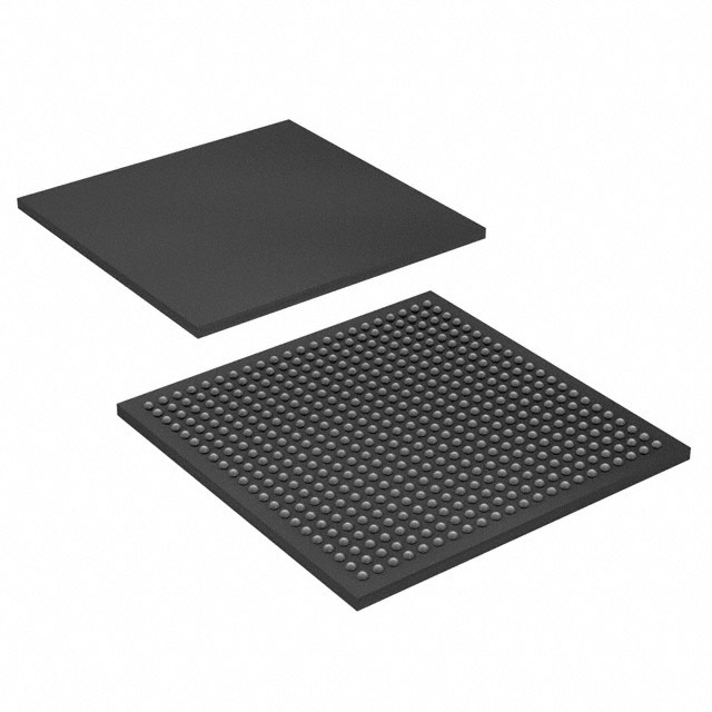
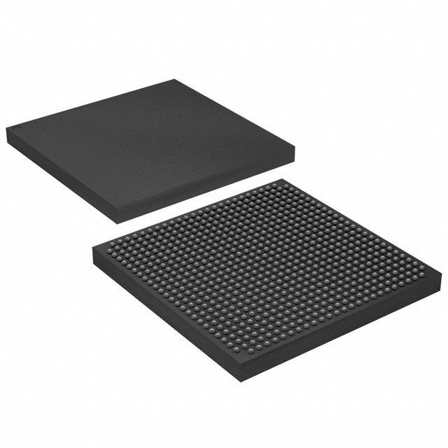
EP2S60F672C3N
| Part Description |
Stratix® II Field Programmable Gate Array (FPGA) IC 492 2544192 60440 672-BBGA |
|---|---|
| Quantity | 198 Available (as of June 14, 2026) |

| Product Category | Field Programmable Gate Array (FPGA) |
|---|---|
| Manufacturer | Intel |
| Manufacturing Status | Obsolete |
| Manufacturer Standard Lead Time | Contact Us |
| Datasheet |
Specifications & Environmental
| Device Package | 672-FBGA (27x27) | Grade | Commercial | Operating Temperature | 0°C – 85°C | ||
|---|---|---|---|---|---|---|---|
| Package / Case | 672-BBGA | Number of I/O | 492 | Voltage | 1.15 V - 1.25 V | ||
| Mounting Method | Surface Mount | RoHS Compliance | RoHS Compliant | REACH Compliance | REACH Unaffected | ||
| Moisture Sensitivity Level | 3 (168 Hours) | Number of LABs/CLBs | 3022 | Number of Logic Elements/Cells | 60440 | ||
| Number of Gates | N/A | ECCN | 3A991D | HTS Code | 8542.39.0001 | ||
| Qualification | N/A | Total RAM Bits | 2544192 |
Overview of EP2S60F672C3N – Stratix® II FPGA, 60,440 logic elements, 672‑BBGA
The EP2S60F672C3N is an Intel Stratix® II field‑programmable gate array packaged in a 672‑BBGA (supplier package: 672‑FBGA, 27×27). It integrates 60,440 logic elements across 3,022 logic array blocks and approximately 2.54 Mbits of embedded RAM, with 492 user I/O pins for broad system interfacing.
Designed for complex digital designs requiring dense programmable logic, on‑chip memory and extensive I/O, this commercial‑grade device supports a 1.15 V to 1.25 V core supply and operates across a 0 °C to 85 °C temperature range. The device is RoHS compliant.
Key Features
- Logic Fabric – 60,440 logic elements implemented across 3,022 logic array blocks to support high‑density programmable logic designs.
- Embedded Memory – Approximately 2.54 Mbits of on‑chip RAM (TriMatrix memory architecture referenced in device handbook) for local data storage and buffering.
- I/O Capacity – 492 user I/O pins and support for advanced I/O structures including double data rate I/O and multi‑volt I/O interfaces as described in the device handbook.
- Clocking & PLLs – Dedicated PLL and hierarchical/global clock network support for flexible clock management and high‑performance timing architectures.
- DSP & Dedicated Blocks – Device handbook references digital signal processing blocks and dedicated circuitry to assist in implementation of arithmetic and signal‑processing functions.
- Configuration & Debug – IEEE 1149.1 JTAG boundary‑scan support and SignalTap II embedded logic analyzer support for in‑system debugging and configuration control.
- System Reliability Features – Hot‑socketing capabilities and power‑on reset circuitry are documented for controlled bring‑up and system integration scenarios.
- Package & Electrical – 672‑BBGA package (supplier: 672‑FBGA, 27×27) with 1.15 V–1.25 V core supply voltage; commercial operating temperature range of 0 °C to 85 °C.
- Compliance – RoHS compliant for regulatory compliance in many commercial applications.
Typical Applications
- High‑performance DSP systems – Use the device’s DSP blocks and dense logic fabric to implement filtering, transforms and custom signal processing pipelines.
- Custom interface bridging – Leverage 492 I/O pins and DDR/multi‑volt I/O support to implement protocol bridging, serialization/deserialization and memory interface logic.
- Embedded packet processing and buffering – On‑chip RAM capacity and flexible logic resources support packet buffering, classification and flow control in networked systems.
- Prototyping complex digital systems – Rich clocking, JTAG boundary‑scan and SignalTap II support enable development, debugging and validation of complex FPGA‑based prototypes.
Unique Advantages
- High logic density: 60,440 logic elements provide the capacity to implement large, complex logic functions on a single device, reducing board‑level component count.
- Substantial on‑chip memory: Approximately 2.54 Mbits of embedded RAM enables local buffering and state storage without external memory for many use cases.
- Extensive I/O flexibility: 492 I/O pins and documented support for advanced I/O modes allow diverse peripheral and high‑speed interface connectivity.
- Robust clocking and DSP support: Integrated PLLs, hierarchical clock networks and DSP blocks documented in the device handbook simplify implementation of timing‑sensitive and compute‑intensive functions.
- Designed for system integration: Hot‑socketing features, power‑on reset circuitry, JTAG boundary‑scan and embedded logic analysis support ease board‑level integration and bring‑up.
- Commercial temperature and RoHS compliance: Operates across 0 °C to 85 °C and meets RoHS requirements for commercial deployments.
Why Choose EP2S60F672C3N?
The EP2S60F672C3N combines a high count of logic elements, substantial embedded RAM and a large I/O complement in a compact 672‑BBGA package, making it suitable for designs that require on‑chip resources and flexible interfacing without relying on external logic. The Stratix II device handbook documents architecture elements such as DSP blocks, TriMatrix memory, PLLs and advanced I/O, providing a clear technical foundation for complex digital, signal processing and interface applications.
This device suits engineering teams building commercial‑grade FPGA solutions that need dense programmable logic, integrated memory and comprehensive configuration and debug capabilities. The Intel Stratix II family documentation included with the device supports implementation, verification and system integration across the product lifecycle.
Request a quote or submit an inquiry to obtain pricing and availability for EP2S60F672C3N and begin evaluating this Stratix® II FPGA for your next design.


Date Founded: 1968
Headquarters: Santa Clara, California, USA
Employees: 130,000+
Revenue: $54.23 Billion
Certifications and Memberships: ISO9001:2015, ISO14001:2015, ISO17025:2017, ISO27001:2022, ISO45001:2018, ISO50001:2018


