
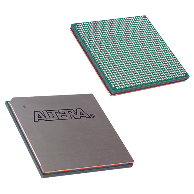
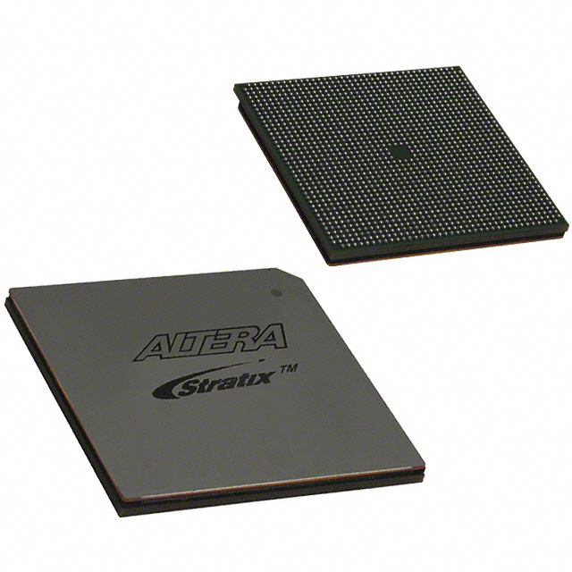
EP2S90F1508C3N
| Part Description |
Stratix® II Field Programmable Gate Array (FPGA) IC 902 4520488 90960 1508-BBGA, FCBGA |
|---|---|
| Quantity | 1,177 Available (as of June 15, 2026) |

| Product Category | Field Programmable Gate Array (FPGA) |
|---|---|
| Manufacturer | Intel |
| Manufacturing Status | Obsolete |
| Manufacturer Standard Lead Time | Contact Us |
| Datasheet |
Specifications & Environmental
| Device Package | 1508-FBGA, FC (40x40) | Grade | Commercial | Operating Temperature | 0°C – 85°C | ||
|---|---|---|---|---|---|---|---|
| Package / Case | 1508-BBGA, FCBGA | Number of I/O | 902 | Voltage | 1.15 V - 1.25 V | ||
| Mounting Method | Surface Mount | RoHS Compliance | RoHS Compliant | REACH Compliance | REACH Unaffected | ||
| Moisture Sensitivity Level | 3 (168 Hours) | Number of LABs/CLBs | 4548 | Number of Logic Elements/Cells | 90960 | ||
| Number of Gates | N/A | ECCN | 3A001A7A | HTS Code | 8542.39.0001 | ||
| Qualification | N/A | Total RAM Bits | 4520488 |
Overview of EP2S90F1508C3N – Stratix® II FPGA — 90,960 Logic Elements, 1508‑FBGA
The EP2S90F1508C3N is a Stratix® II family field programmable gate array (FPGA) in a 1508‑FBGA surface‑mount package. It provides a high logic capacity with integrated on‑chip memory and a large I/O count for dense, reconfigurable system designs.
Designed for commercial‑grade applications, this device is suited to designs that require substantial logic resources, embedded RAM, and robust I/O capability while operating within a 1.15 V to 1.25 V core supply range and a 0 °C to 85 °C temperature window.
Key Features
- Logic Capacity — 90,960 logic elements arranged across 4,548 logic array blocks (LABs) to implement complex programmable logic functions.
- Embedded Memory — 4,520,488 total RAM bits (approximately 4.52 Mbits) of on‑chip memory for FIFOs, buffers, and local data storage.
- High I/O Density — 902 I/O pins to support extensive peripheral interfacing and multi‑lane signaling.
- Power and Thermal — Core voltage supply 1.15 V to 1.25 V; commercial operating temperature range 0 °C to 85 °C.
- Package & Mounting — 1508‑BBGA (FCBGA) supplier package 1508‑FBGA, FC (40×40); surface‑mount mounting for standard PCB assembly.
- Stratix II Family Architecture — Device handbook coverage includes advanced architecture elements such as adaptive logic modules, DSP blocks, multi‑track interconnect, PLLs and clock networks, and TriMatrix memory organization.
- Configuration & Debugging — Family documentation references support for IEEE‑1149.1 JTAG boundary‑scan and embedded debug features such as SignalTap II logic analysis and multiple configuration schemes.
- I/O and Interface Features — Family‑level capabilities include high‑speed differential I/O, double data rate I/O support, programmable drive strengths, on‑chip termination and multi‑VOLT I/O interface options as documented for Stratix II devices.
- Regulatory — RoHS compliant.
Typical Applications
- High‑Performance Signal Processing — Use the Stratix II device family’s DSP blocks and large logic fabric to implement filters, transforms, and other compute‑intensive data paths.
- Memory Interface & Bridging — On‑chip RAM and documented external memory interfacing support make this device suitable for memory controller and bridging functions.
- High‑Density I/O Systems — The 902 I/O pins support multi‑lane connectivity, high‑speed differential signaling and complex board‑level I/O requirements.
- Prototyping & Embedded Logic Analysis — Built‑in JTAG boundary‑scan and SignalTap II family features facilitate board bring‑up and in‑system debugging.
Unique Advantages
- Substantial Logic Resources: 90,960 logic elements and 4,548 LABs provide significant capacity for large FPGA designs without external logic.
- Embedded Memory On‑Board: Approximately 4.52 Mbits of RAM reduces dependency on external memory for many buffering and storage tasks.
- Extensive I/O Count: 902 I/Os enable complex multi‑interface designs and high signal routing density on a single device.
- Comprehensive Family Documentation: Stratix II device handbook covers architecture, timing, PLLs, I/O standards, configuration and test features to support design and verification.
- Commercial‑Grade Reliability: Specified operating range (0 °C to 85 °C) and RoHS compliance meet standard commercial product requirements.
- Standard Package for Production: 1508‑FBGA surface‑mount package (40×40) supports established PCB assembly processes for volume manufacturing.
Why Choose EP2S90F1508C3N?
The EP2S90F1508C3N delivers a balanced combination of large logic capacity, substantial embedded RAM, and extensive I/O in a commercial‑grade Stratix II FPGA package. It is well suited for engineers developing complex signal processing, memory interfacing, and high‑I/O designs that require a mature device family with extensive architectural and configuration documentation.
Choose this device when you need on‑chip resources to reduce external components, flexible I/O to accommodate multiple interfaces, and Stratix II family features such as PLLs, DSP blocks, and embedded debugging capabilities to streamline development and verification.
Request a quote or submit an inquiry for EP2S90F1508C3N to obtain pricing and availability information.


Date Founded: 1968
Headquarters: Santa Clara, California, USA
Employees: 130,000+
Revenue: $54.23 Billion
Certifications and Memberships: ISO9001:2015, ISO14001:2015, ISO17025:2017, ISO27001:2022, ISO45001:2018, ISO50001:2018


