
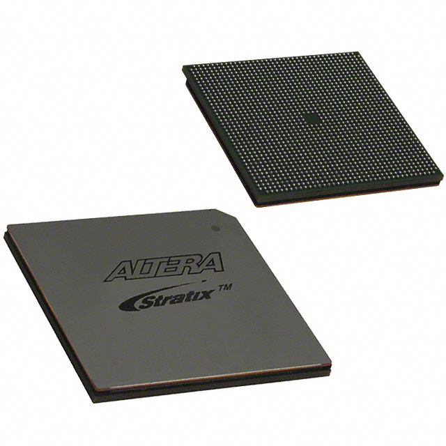
EP2S90F1508C5
| Part Description |
Stratix® II Field Programmable Gate Array (FPGA) IC 902 4520488 90960 1508-BBGA, FCBGA |
|---|---|
| Quantity | 1,233 Available (as of June 14, 2026) |
| Product Category | Field Programmable Gate Array (FPGA) |
|---|---|
| Manufacturer | Intel |
| Manufacturing Status | Obsolete |
| Manufacturer Standard Lead Time | Contact Us |
| Datasheet |
Specifications & Environmental
| Device Package | 1508-FBGA, FC (40x40) | Grade | Commercial | Operating Temperature | 0°C – 85°C | ||
|---|---|---|---|---|---|---|---|
| Package / Case | 1508-BBGA, FCBGA | Number of I/O | 902 | Voltage | 1.15 V - 1.25 V | ||
| Mounting Method | Surface Mount | RoHS Compliance | RoHS non-compliant | REACH Compliance | REACH Unaffected | ||
| Moisture Sensitivity Level | 3 (168 Hours) | Number of LABs/CLBs | 4548 | Number of Logic Elements/Cells | 90960 | ||
| Number of Gates | N/A | ECCN | 3A001A7A | HTS Code | 8542.39.0001 | ||
| Qualification | N/A | Total RAM Bits | 4520488 |
Overview of EP2S90F1508C5 – Stratix II FPGA, 1508-FBGA (40×40)
The EP2S90F1508C5 is a Stratix® II Field Programmable Gate Array (FPGA) in a 1508-ball FBGA package intended for commercial-temperature applications. It combines high logic density, embedded memory, and extensive I/O to address complex digital integration, signal processing, and high‑I/O interface designs.
Built on the Stratix II device family architecture described in the device handbook, this part targets designs that require large amounts of programmable logic, dedicated DSP resources, flexible clocking (PLLs), and comprehensive I/O support.
Key Features
- High Logic Density — 90,960 logic elements for implementing large state machines, glue logic, and custom datapaths.
- Embedded Memory — Approximately 4.52 Mbits of on-chip RAM (4,520,488 total RAM bits) for FIFOs, buffering, and on-chip data storage.
- Extensive I/O — 902 I/O pins to support wide external bus interfaces and multi-channel connectivity; datasheet includes high-speed I/O and DDR I/O specifications.
- Clocking & PLLs — Stratix II device architecture includes PLL and global/hierarchical clock network support for flexible timing and multi-clock systems.
- DSP & Processing Blocks — Family documentation details dedicated DSP block support for signal processing tasks and arithmetic acceleration.
- Package & Mounting — 1508-BBGA / 1508-FBGA (40×40) surface-mount package for compact, board-level integration.
- Power — Core supply voltage range of 1.15 V to 1.25 V to match targeted system power rails.
- Commercial Grade & Temperature Range — Rated for commercial operation from 0 °C to 85 °C.
- Compliance & Testability — RoHS-compliant; family documentation includes JTAG boundary-scan and embedded logic analysis (SignalTap II) support for debug and validation.
Typical Applications
- High-Density Digital Systems — Implement large combinational and sequential logic, state machines, and glue logic where tens of thousands of logic elements are required.
- Digital Signal Processing — Use the device’s DSP block support and embedded memory for filtering, modulation, and other signal-processing pipelines.
- High‑Bandwidth Interfaces — Leverage 902 I/O pins and the Stratix II I/O architecture for wide parallel interfaces, DDR links, and multi‑lane data paths.
- Prototyping & System Integration — Integrate complex subsystems and verify multi-clock designs using the device family’s PLLs and on‑chip debugging capabilities.
Unique Advantages
- Highly integrated logic and memory: 90,960 logic elements paired with approximately 4.52 Mbits of on‑chip RAM reduces the need for external components and simplifies board design.
- Very high I/O count: 902 I/O pins enable broad external connectivity and flexible interface implementations without multiplexing compromises.
- Flexible clocking infrastructure: Built-in PLL and hierarchical clock networks support complex multi-domain timing architectures and clock management.
- Surface-mount, compact package: 1508-FBGA (40×40) allows dense PCB implementations while providing the pin-count needed for high-throughput systems.
- Commercial temperature suitability: Designed for 0 °C to 85 °C operation to meet standard commercial application requirements.
- Debug and validation features: Family documentation highlights JTAG and embedded logic analyzer capabilities that help accelerate bring-up and troubleshooting.
Why Choose EP2S90F1508C5?
The EP2S90F1508C5 positions itself as a high-density Stratix II FPGA option for designs that require substantial programmable logic, embedded memory, and a large number of I/O pins within a compact FBGA footprint. Its documented family features—DSP blocks, PLLs, multi-track interconnect, and on‑chip memory—make it suitable for complex digital, signal-processing, and interface-centric designs at commercial temperatures.
Choose this device when your design needs a combination of logic capacity, embedded RAM, and flexible clocking/I/O resources, backed by the Stratix II device handbook and family documentation for design, configuration, and test guidance.
Request a quote or submit a product inquiry to receive pricing and availability information for the EP2S90F1508C5.


Date Founded: 1968
Headquarters: Santa Clara, California, USA
Employees: 130,000+
Revenue: $54.23 Billion
Certifications and Memberships: ISO9001:2015, ISO14001:2015, ISO17025:2017, ISO27001:2022, ISO45001:2018, ISO50001:2018


