
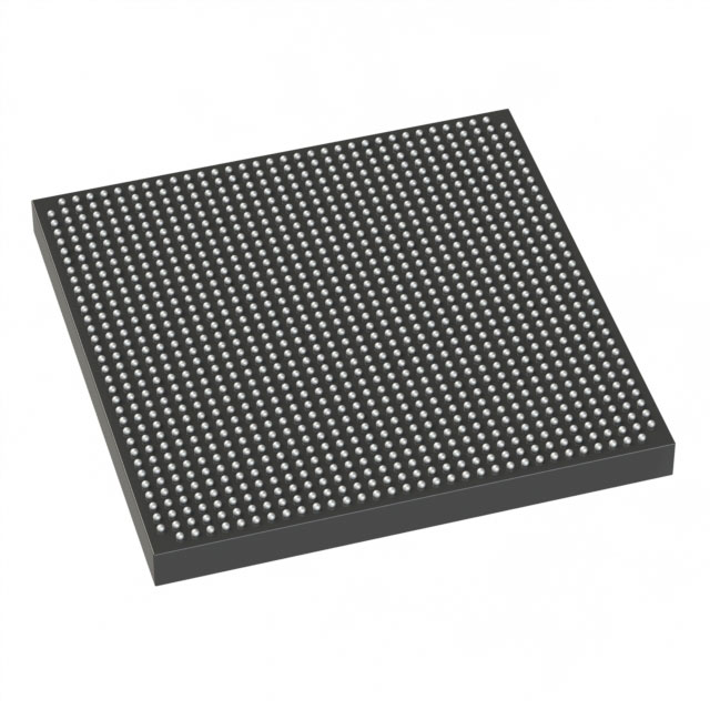
EP2SGX90EF1152C3
| Part Description |
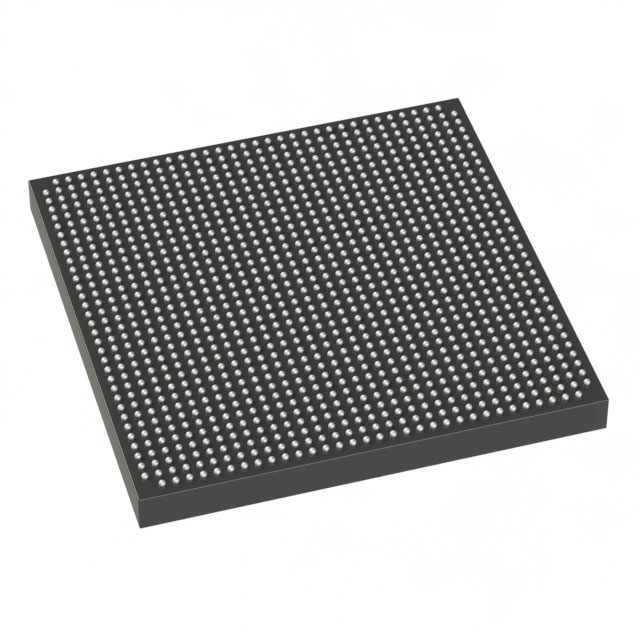
Stratix® II GX Field Programmable Gate Array (FPGA) IC 558 4520448 90960 1152-BBGA |
|---|---|
| Quantity | 284 Available (as of October 8, 2026) |
| Product Category | Field Programmable Gate Array (FPGA) |
|---|---|
| Manufacturer | Intel |
| Manufacturing Status | Obsolete |
| Manufacturer Standard Lead Time | Contact Us |
| Datasheet |
Specifications & Environmental
| Device Package | 1152-FBGA (35x35) | Grade | Commercial | Operating Temperature | 0°C – 85°C | ||
|---|---|---|---|---|---|---|---|
| Package / Case | 1152-BBGA | Number of I/O | 558 | Voltage | 1.15 V - 1.25 V | ||
| Mounting Method | Surface Mount | RoHS Compliance | RoHS Compliant | REACH Compliance | REACH Unaffected | ||
| Moisture Sensitivity Level | 3 (168 Hours) | Number of LABs/CLBs | 4548 | Number of Logic Elements/Cells | 90960 | ||
| Number of Gates | N/A | ECCN | 3A001A2C | HTS Code | 8542.39.0001 | ||
| Qualification | N/A | Total RAM Bits | 4520448 |
Overview of EP2SGX90EF1152C3 – Stratix® II GX FPGA, 1152‑BBGA
The EP2SGX90EF1152C3 is an Intel Stratix® II GX field‑programmable gate array in a 1152‑BBGA package, designed for high‑performance logic and system integration. It delivers a large logic fabric alongside substantial embedded memory and high I/O density, making it suitable for communications, protocol bridging, and high‑speed interface applications.
As a member of the Stratix II GX family, the device aligns with the family’s architecture that combines a scalable logic array with high‑speed serial transceiver technology and advanced clocking and DSP resources referenced in the device datasheet.
Key Features
- Logic Capacity — 90,960 logic elements for implementing complex digital systems and deep custom logic.
- Embedded Memory — Approximately 4.52 Mbits of on‑chip RAM to support FIFOs, buffers, and data‑intensive processing.
- I/O Density — 558 user I/O pins to accommodate wide parallel interfaces and high‑channel connectivity.
- Family Transceiver Capabilities (Stratix II GX) — The Stratix II GX family provides high‑speed serial transceivers supporting 600 Mbps to 6.375 Gbps per channel and multi‑protocol operation, as described in the device series documentation.
- Clocking & PLLs (Series) — Stratix II GX architecture includes enhanced PLL resources for spread spectrum, programmable bandwidth, and real‑time reconfiguration (series‑level capability described in the datasheet).
- DSP & Performance (Series) — The family includes high‑speed DSP blocks suitable for multipliers, MACs, and FIR implementations (series‑level capability described in the datasheet).
- Package & Mounting — 1152‑BBGA (supplier package listed as 1152‑FBGA, 35 × 35 mm) in a surface‑mount format for compact board integration.
- Power — Core supply range specified at 1.15 V to 1.25 V for device operation.
- Operating Range & Grade — Commercial grade device with an operating temperature range of 0 °C to 85 °C.
- Compliance — RoHS‑compliant.
Typical Applications
- High‑speed backplane and switch fabrics — Leverages large logic capacity and high I/O count for packet routing, table lookup, and interface bridging tasks.
- Communications protocol bridging — Family transceiver capabilities and abundant logic enable implementation of protocol converters and link adapters.
- Chip‑to‑chip interfaces and board‑level aggregation — High I/O density and embedded memory support wide parallel buses, buffering, and data aggregation between components.
- Accelerated signal processing — Significant logic and on‑chip RAM support custom DSP pipelines and buffering for data‑plane processing.
Unique Advantages
- High logic density: 90,960 logic elements provide the capacity needed for complex functions and integration of multiple subsystems into a single device.
- Substantial embedded memory: Approximately 4.52 Mbits of on‑chip RAM reduces external memory dependence for many buffering and FIFO use cases.
- Extensive I/O: 558 I/O pins let you implement wide parallel interfaces and support multi‑channel connectivity without external expanders.
- Surface‑mount BGA package: 1152‑BBGA / 1152‑FBGA (35 × 35 mm) balances board area and routing density for mid‑to‑high complexity PCBs.
- Series‑level high‑speed transceivers: Stratix II GX family transceiver architecture supports multi‑Gbps serial links for demanding link and protocol applications (series reference).
- Commercial thermal profile: 0 °C to 85 °C rating matches standard commercial electronics environments and system‑level design expectations.
Why Choose EP2SGX90EF1152C3?
The EP2SGX90EF1152C3 positions itself as a high‑capacity, integration‑focused FPGA for designs that require large logic resources, significant embedded memory, and high I/O count in a compact BGA footprint. Its alignment with the Stratix II GX family architecture brings series‑level capabilities such as advanced transceivers, DSP resources, and flexible clocking to systems where throughput and interface density matter.
This device is well suited to engineering teams building communications equipment, high‑speed interface bridges, and board‑level aggregation solutions that benefit from a single, programmable device to consolidate functions, reduce BOM complexity, and accelerate time to prototype.
Request a quote or submit an RFQ for EP2SGX90EF1152C3 to receive pricing and availability information.





















Date Founded: 1968
Headquarters: Santa Clara, California, USA
Employees: 130,000+
Revenue: $54.23 Billion
Certifications and Memberships: ISO9001:2015, ISO14001:2015, ISO17025:2017, ISO27001:2022, ISO45001:2018, ISO50001:2018


