
EP2SGX90EF1152C5ES
| Part Description |
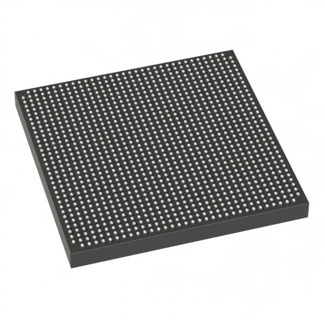
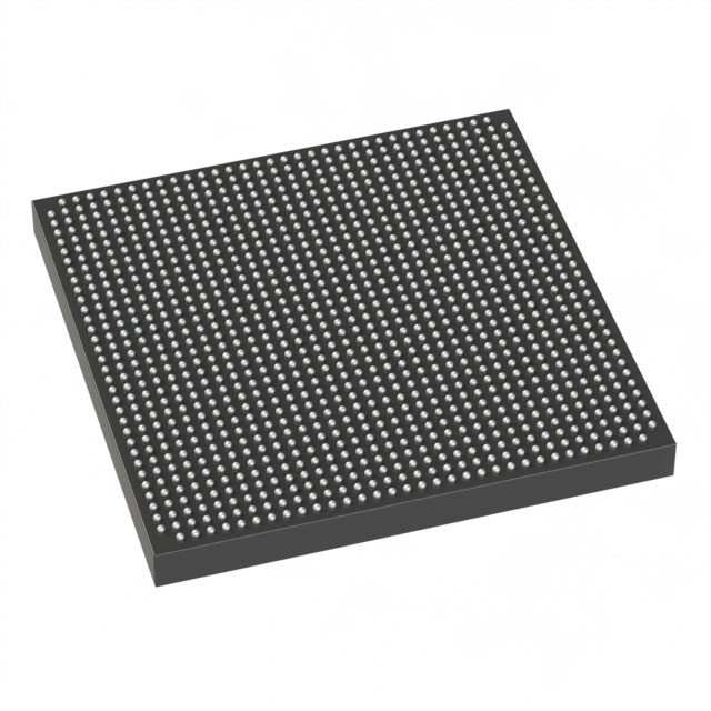
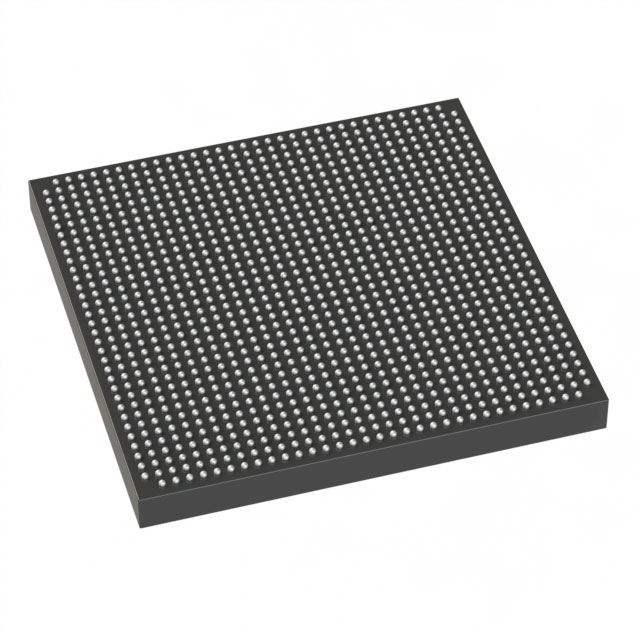
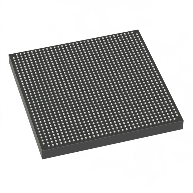
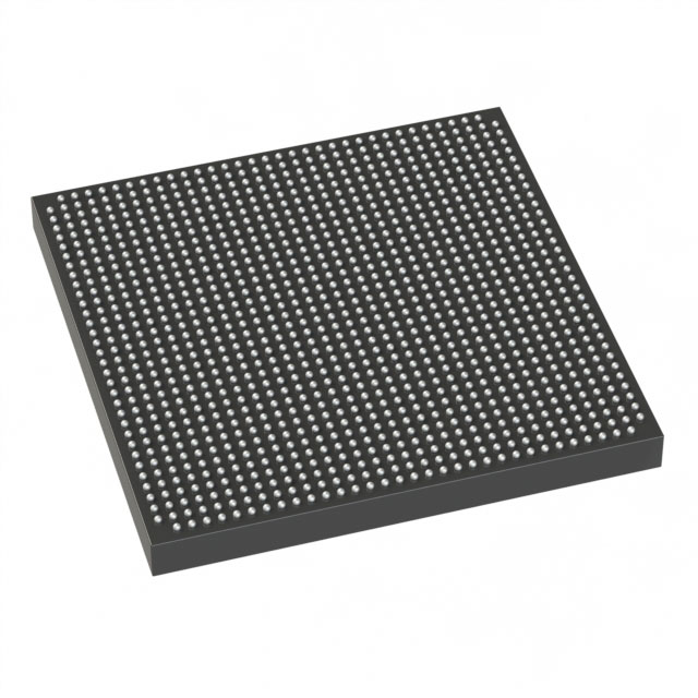
Stratix® II GX Field Programmable Gate Array (FPGA) IC 558 4520448 90960 1152-BBGA |
|---|---|
| Quantity | 1,662 Available (as of October 8, 2026) |

| Product Category | Field Programmable Gate Array (FPGA) |
|---|---|
| Manufacturer | Intel |
| Manufacturing Status | Obsolete |
| Manufacturer Standard Lead Time | Contact Us |
| Datasheet |
Specifications & Environmental
| Device Package | 1152-FBGA (35x35) | Grade | Commercial | Operating Temperature | 0°C – 85°C | ||
|---|---|---|---|---|---|---|---|
| Package / Case | 1152-BBGA | Number of I/O | 558 | Voltage | 1.15 V - 1.25 V | ||
| Mounting Method | Surface Mount | RoHS Compliance | RoHS non-compliant | REACH Compliance | REACH Unaffected | ||
| Moisture Sensitivity Level | 3 (168 Hours) | Number of LABs/CLBs | 4548 | Number of Logic Elements/Cells | 90960 | ||
| Number of Gates | N/A | ECCN | 3A001A7A | HTS Code | 8542.39.0001 | ||
| Qualification | N/A | Total RAM Bits | 4520448 |
Overview of EP2SGX90EF1152C5ES – Stratix® II GX Field Programmable Gate Array (FPGA) IC 558 4520448 90960 1152-BBGA
The EP2SGX90EF1152C5ES is a commercial-grade Stratix® II GX FPGA from Intel, built on a high-performance, scalable logic architecture that combines a dense logic array with the Stratix II GX transceiver ecosystem. With 90,960 logic elements, approximately 4.52 Mbits of embedded memory and 558 user I/O, this device targets demanding communications, networking and protocol-bridging designs that require high I/O density and flexible serial connectivity.
Based on the Stratix II GX family architecture, the device benefits from integrated high-speed serial transceiver technology, multi-level on-chip RAM, and advanced clocking resources—enabling system designers to address high-bandwidth backplane, chip-to-chip and communications interface applications while operating at low core voltages.
Key Features
- Logic Capacity 90,960 logic elements for implementing complex digital designs and large custom logic functions.
- Embedded Memory Approximately 4.52 Mbits of on-chip RAM to support FIFOs, buffers and memory-intensive algorithms.
- I/O Density 558 user I/O pins to support wide parallel interfaces and flexible board-level connectivity.
- High‑Speed Transceiver Architecture Stratix II GX family transceiver technology supports clock-and-data recovery and SERDES operation from 600 Mbps up to 6.375 Gbps per channel (family specification), enabling high-bandwidth serial links and protocol support.
- Clocking and DSP Architecture includes multiple global and regional clock networks, enhanced PLLs with reconfiguration capability, and dedicated DSP/multiplier resources suitable for high-speed signal processing (family features).
- TriMatrix Memory Architecture Three RAM block sizes (family feature) provide flexible true dual-port memory and FIFO implementations with high performance.
- Power and Voltage Core voltage supply range: 1.15 V to 1.25 V for low-voltage system designs; supports per-channel power-down for reduced consumption (transceiver family feature).
- Commercial Temperature Range Rated for 0 °C to 85 °C operation; device grade: Commercial.
- Package & Mounting 1152-BBGA package (supplier device package: 1152-FBGA, 35 × 35 mm) with surface-mount assembly for high-density PCB layouts.
- Regulatory RoHS compliant.
Typical Applications
- High‑speed Networking Equipment Implement packet processing, protocol bridging and backplane interfaces using the device’s dense logic, embedded memory and family transceiver capabilities.
- Communications Protocol Conversion Translate between serial protocols and parallel buses or aggregate multiple serial links using the Stratix II GX transceiver and FPGA fabric.
- Chip‑to‑Chip Interconnect Use high I/O counts and SERDES-enabled links for board-level or board-to-board high-bandwidth interconnects.
- Signal Processing and DSP Acceleration Leverage on-chip RAM and DSP resources for filtering, accumulation and other high-speed signal-processing tasks (family features).
Unique Advantages
- High logic density: 90,960 logic elements provide headroom for complex designs and custom IP integration.
- Substantial embedded memory: Approximately 4.52 Mbits of on-chip RAM reduces external memory requirements and simplifies buffer/FIFO implementations.
- Extensive I/O: 558 user I/O pins enable broad peripheral connectivity and support for wide parallel interfaces.
- Low-voltage core operation: 1.15–1.25 V supply supports modern low-voltage system architectures and power-optimized designs.
- Stratix II GX transceiver technology: Family-level support for high-speed serial links and CDR/SERDES capabilities enables flexible, high-bandwidth interfacing.
- RoHS compliant and surface-mount package: Meets environmental compliance requirements and supports compact PCB assembly in a 1152-BBGA form factor.
Why Choose EP2SGX90EF1152C5ES?
The EP2SGX90EF1152C5ES brings a combination of high logic capacity, multi-megabit embedded memory, and abundant I/O in a single commercial‑grade Stratix II GX FPGA package. Its architecture—rooted in the Stratix II GX device family—aligns with designs that require integrated high-speed serial functionality alongside large programmable fabric and memory resources.
This device is well suited for teams developing high-bandwidth communications, backplane and protocol-bridging systems that need scalable logic, on-chip memory and flexible transceiver technology while operating within commercial temperature limits. The platform’s documented architecture and family-level features support long-term design scalability and integration into established development flows.
Request a quote or submit a request for pricing and availability to begin evaluating EP2SGX90EF1152C5ES for your next design.
























Date Founded: 1968
Headquarters: Santa Clara, California, USA
Employees: 130,000+
Revenue: $54.23 Billion
Certifications and Memberships: ISO9001:2015, ISO14001:2015, ISO17025:2017, ISO27001:2022, ISO45001:2018, ISO50001:2018


