
EP2SGX90EF1152C5N
| Part Description |
Stratix® II GX Field Programmable Gate Array (FPGA) IC 558 4520448 90960 1152-BBGA |
|---|---|
| Quantity | 500 Available (as of June 16, 2026) |

| Product Category | Field Programmable Gate Array (FPGA) |
|---|---|
| Manufacturer | Intel |
| Manufacturing Status | Obsolete |
| Manufacturer Standard Lead Time | Contact Us |
| Datasheet |
Specifications & Environmental
| Device Package | 1152-FBGA (35x35) | Grade | Commercial | Operating Temperature | 0°C – 85°C | ||
|---|---|---|---|---|---|---|---|
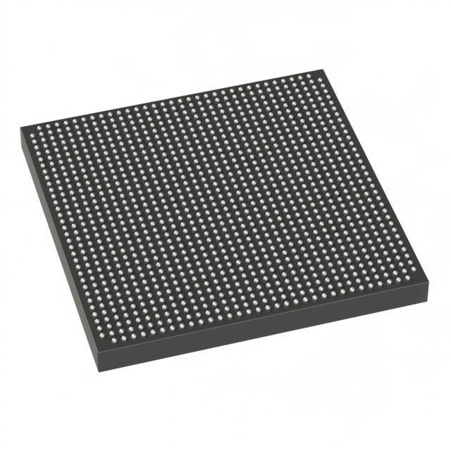
| Package / Case | 1152-BBGA | Number of I/O | 558 | Voltage | 1.15 V - 1.25 V | ||
| Mounting Method | Surface Mount | RoHS Compliance | RoHS Compliant | REACH Compliance | REACH Unaffected | ||
| Moisture Sensitivity Level | 3 (168 Hours) | Number of LABs/CLBs | 4548 | Number of Logic Elements/Cells | 90960 | ||
| Number of Gates | N/A | ECCN | 3A001A7A | HTS Code | 8542.39.0001 | ||
| Qualification | N/A | Total RAM Bits | 4520448 |
Overview of EP2SGX90EF1152C5N – Stratix® II GX Field Programmable Gate Array (FPGA) IC 558 4520448 90960 1152-BBGA
The EP2SGX90EF1152C5N is a Stratix® II GX family FPGA from Intel, combining a scalable high‑performance logic array with the Stratix II GX series’ advanced serial-transceiver architecture. This device targets designs that require dense programmable logic, substantial on-chip memory, and flexible high-speed I/O connectivity.
Typical markets include high-speed communications, networking and protocol-bridging applications where integrated transceiver capability, robust clocking and DSP resources accelerate time to market and simplify system design.
Key Features
- Logic Capacity — 90,960 logic elements for implementing complex digital functions and system-level logic integration.
- Embedded Memory — Approximately 4.52 Mbits of on-chip RAM (4,520,448 total RAM bits) to support FIFOs, packet buffering and data path storage.
- I/O — 558 user I/O pins providing broad connectivity for parallel and source‑synchronous interfaces.
- High‑Speed Transceiver Architecture — Stratix II GX family transceiver technology supporting high-speed serial protocols (family-level capability up to 6.375 Gbps and multi-channel configurations) for backplane, chip‑to‑chip and serial protocol bridging.
- DSP and Clocking — Family features include high-speed DSP blocks and multiple global/regional clock networks with enhanced PLLs for flexible clocking and accelerated signal processing (family-level capabilities described in the Stratix II GX device handbook).
- Package & Mounting — 1152-BBGA package (supplier package: 1152-FBGA, 35×35 mm) with surface-mount mounting type for compact board integration.
- Power — Core voltage supply 1.15 V to 1.25 V to match system power domains and enable predictable power planning.
- Operating Range — Commercial grade operation from 0 °C to 85 °C; RoHS compliant.
Typical Applications
- High‑Speed Networking Equipment — Implement backplane interfaces and packet processing pipelines using the device’s dense logic, on-chip RAM and Stratix II GX transceiver capabilities.
- Telecom & Data Transport — Support protocol bridging and serial link aggregation leveraging family transceiver features and flexible clocking resources.
- Embedded System Acceleration — Offload compute‑intensive DSP tasks with on‑die DSP blocks and hardware‑accelerated multiply/accumulate functions described for the Stratix II GX family.
- Memory Interface Controllers — Deploy controllers for high‑speed external memories using the embedded RAM and I/O flexibility to implement buffer and timing-critical logic.
Unique Advantages
- High Logic Density: 90,960 logic elements enable consolidation of multiple subsystems into a single FPGA to reduce board-level BOM and interconnect complexity.
- Substantial Embedded Memory: Approximately 4.52 Mbits of on‑chip RAM supports deep FIFOs and buffering without immediate external memory dependence.
- Broad I/O Count: 558 I/O pins provide the capacity to interface with wide parallel buses, multiple high-speed lanes, or dense peripheral sets.
- Stratix II GX Transceiver Technology: Family-level support for multi‑Gbps serial channels and protocol reconfiguration simplifies high-speed link design and enables flexible protocol support.
- Flexible Clocking & DSP Resources: Family features such as multiple global/regional clock networks, enhanced PLLs and DSP blocks facilitate synchronized data paths and real-time signal processing.
- Commercial Grade & RoHS Compliant: Rated for 0 °C to 85 °C operation and compliant with RoHS for regulatory and manufacturing consistency.
Why Choose EP2SGX90EF1152C5N?
The EP2SGX90EF1152C5N positions designers to integrate substantial logic, memory and I/O bandwidth with the Stratix II GX family’s high‑speed transceiver and DSP capabilities. It is suited for teams building high‑throughput networking, communications and embedded acceleration systems that require a balance of programmable density and serial link flexibility.
Backed by Intel’s Stratix II GX device handbook and family megafunction support, this device provides a scalable platform for designs that may evolve over time—helping reduce redevelopment effort through a familiar architecture and available family‑level resources.
Request a quote or submit an availability inquiry to get pricing, lead time and ordering information for EP2SGX90EF1152C5N.


Date Founded: 1968
Headquarters: Santa Clara, California, USA
Employees: 130,000+
Revenue: $54.23 Billion
Certifications and Memberships: ISO9001:2015, ISO14001:2015, ISO17025:2017, ISO27001:2022, ISO45001:2018, ISO50001:2018


