
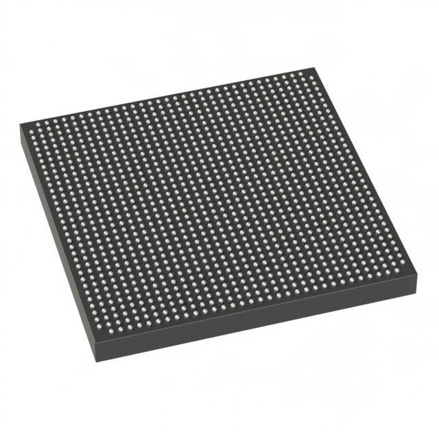
EP2SGX90EF1152I4N
| Part Description |
Stratix® II GX Field Programmable Gate Array (FPGA) IC 558 4520448 90960 1152-BBGA |
|---|---|
| Quantity | 1,348 Available (as of June 10, 2026) |

| Product Category | Field Programmable Gate Array (FPGA) |
|---|---|
| Manufacturer | Intel |
| Manufacturing Status | Obsolete |
| Manufacturer Standard Lead Time | Contact Us |
| Datasheet |
Specifications & Environmental
| Device Package | 1152-FBGA (35x35) | Grade | Industrial | Operating Temperature | -40°C – 100°C | ||
|---|---|---|---|---|---|---|---|
| Package / Case | 1152-BBGA | Number of I/O | 558 | Voltage | 1.15 V - 1.25 V | ||
| Mounting Method | Surface Mount | RoHS Compliance | RoHS Compliant | REACH Compliance | REACH Unaffected | ||
| Moisture Sensitivity Level | 3 (168 Hours) | Number of LABs/CLBs | 4548 | Number of Logic Elements/Cells | 90960 | ||
| Number of Gates | N/A | ECCN | 3A001A2C | HTS Code | 8542.39.0001 | ||
| Qualification | N/A | Total RAM Bits | 4520448 |
Overview of EP2SGX90EF1152I4N – Stratix® II GX FPGA IC, 1152‑BBGA
The EP2SGX90EF1152I4N is a Stratix® II GX field programmable gate array (FPGA) in a 1152‑BBGA package, designed for high‑performance, high‑integration digital systems. Built on the Stratix II GX architecture, this device combines a large logic array with abundant embedded memory and the family’s high‑speed serial transceiver capabilities to address demanding communications, networking and interface bridging applications.
With 90,960 logic elements, approximately 4.52 Mbits of embedded memory, and 558 user I/Os, the device targets designs that require dense programmable logic, extensive on‑chip RAM, and flexible I/O and transceiver options while supporting industrial operating conditions.
Key Features
- Logic Density 90,960 logic elements provide substantial programmable fabric for complex digital designs and system integration.
- Embedded Memory (TriMatrix) Approximately 4.52 Mbits of on‑chip RAM using TriMatrix memory architecture, enabling true dual‑port memory and high‑performance FIFO implementations.
- High‑Speed Serial Transceivers (family capability) Stratix II GX devices include high‑speed serial transceiver channels with embedded SERDES and clock/data recovery, supporting protocol rates from 600 Mbps up to 6.375 Gbps per channel for serial links and protocol bridging.
- I/O and Interface Flexibility 558 user I/Os with support for a wide range of single‑ended and differential standards and up to 71 channels of high‑speed source‑synchronous differential I/O (family capability).
- DSP and Clocking Resources Device family includes high‑speed DSP blocks for dedicated multipliers and MAC functions and up to four enhanced PLLs for advanced clock management and dynamic reconfiguration.
- Power and Supply Core voltage supply range of 1.15 V to 1.25 V to match system power delivery requirements.
- Package and Mounting 1152‑BBGA (supplier package: 1152‑FBGA, 35×35 mm) surface‑mount package for high‑density PCB designs.
- Industrial Temperature Grade Rated for operation from −40 °C to 100 °C and RoHS compliant for industrial deployments.
Typical Applications
- High‑Speed Networking Implementation of backplane interfaces, protocol bridging, and packet processing using the device’s large logic array, embedded memory, and high‑speed serial channels.
- Telecommunications Equipment Serial link aggregation, SONET/SDH, CPRI and other transport protocols where SerDes and clock/data recovery are required.
- Video and Broadcast Systems Support for SDI and other high‑bandwidth video interfaces leveraging the family’s transceiver throughput and on‑chip memory for buffering and processing.
- High‑Performance System Interconnect Chip‑to‑chip bridging and high‑speed external memory interfaces (DDR/QDR family support noted in device family documentation) for complex boards and mezzanine modules.
Unique Advantages
- High logic capacity: 90,960 logic elements enable integration of large custom logic functions and IP cores on a single device.
- Substantial on‑chip RAM: Approximately 4.52 Mbits of embedded memory supports FIFOs, buffering, and memory‑intensive algorithms without immediate need for external RAM.
- Integrated serial transceiver technology: Family transceivers with embedded SERDES and clock/data recovery simplify implementation of multi‑Gbps links and reduce external component count.
- Robust industrial operation: −40 °C to 100 °C rating and RoHS compliance make the device suitable for industrial electronic systems.
- Flexible package density: The 1152‑BBGA (35×35 mm) package delivers high I/O count and dense routing for complex PCBs.
- Advanced clocking and DSP support: Enhanced PLLs and on‑die DSP blocks provide native resources for high‑speed signal processing and precise timing control.
Why Choose EP2SGX90EF1152I4N?
The EP2SGX90EF1152I4N positions itself as a high‑capacity Stratix II GX FPGA option for designs that require extensive programmable logic, significant embedded memory, and family‑level high‑speed transceiver capabilities. Its combination of logic density, memory resources, abundant I/Os, and industrial temperature rating makes it suitable for networking, telecom, broadcast, and other high‑performance embedded systems.
Designers benefit from a device that consolidates multiple system functions into a single programmable device, offering scalability through the Stratix II GX family architecture and support for advanced clocking, DSP functions, and serial protocol options documented for the series.
If you would like pricing, availability, or to request a formal quote for EP2SGX90EF1152I4N, submit a request and our team will respond with detailed purchasing information and lead‑time guidance.


Date Founded: 1968
Headquarters: Santa Clara, California, USA
Employees: 130,000+
Revenue: $54.23 Billion
Certifications and Memberships: ISO9001:2015, ISO14001:2015, ISO17025:2017, ISO27001:2022, ISO45001:2018, ISO50001:2018


