
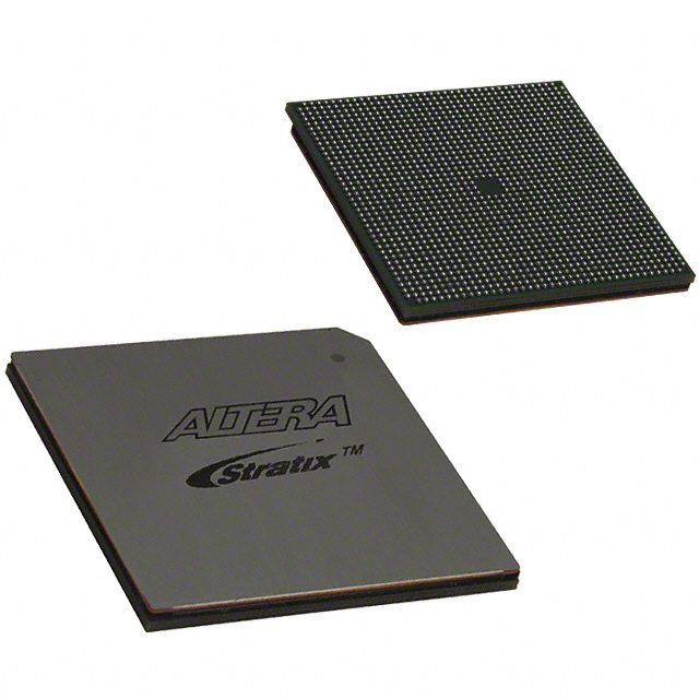
EP2SGX90FF1508C4N
| Part Description |
Stratix® II GX Field Programmable Gate Array (FPGA) IC 650 4520448 90960 1508-BBGA, FCBGA |
|---|---|
| Quantity | 1,121 Available (as of June 10, 2026) |

| Product Category | Field Programmable Gate Array (FPGA) |
|---|---|
| Manufacturer | Intel |
| Manufacturing Status | Obsolete |
| Manufacturer Standard Lead Time | Contact Us |
| Datasheet |
Specifications & Environmental
| Device Package | 1508-FBGA, FC (40x40) | Grade | Commercial | Operating Temperature | 0°C – 85°C | ||
|---|---|---|---|---|---|---|---|
| Package / Case | 1508-BBGA, FCBGA | Number of I/O | 650 | Voltage | 1.15 V - 1.25 V | ||
| Mounting Method | Surface Mount | RoHS Compliance | RoHS Compliant | REACH Compliance | REACH Unaffected | ||
| Moisture Sensitivity Level | 3 (168 Hours) | Number of LABs/CLBs | 4548 | Number of Logic Elements/Cells | 90960 | ||
| Number of Gates | N/A | ECCN | 3A001A7A | HTS Code | 8542.39.0001 | ||
| Qualification | N/A | Total RAM Bits | 4520448 |
Overview of EP2SGX90FF1508C4N – Stratix® II GX FPGA, 90,960 Logic Elements, 1508‑BBGA
The EP2SGX90FF1508C4N is an Intel Stratix® II GX field-programmable gate array in a 1508‑ball BGA package designed for high-performance, I/O‑dense systems. Built on the Stratix II GX architecture, it combines a large logic array, multi-megabit embedded memory, and family-level high-speed serial transceiver capabilities aimed at communications, backplane, and complex protocol-bridging applications.
This commercial‑grade, surface‑mount device delivers 90,960 logic elements, approximately 4.52 Mbits of on‑chip RAM, and 650 I/Os, with a nominal supply range of 1.15–1.25 V and an operating temperature range of 0 °C to 85 °C.
Key Features
- Logic Capacity 90,960 logic elements suitable for large FPGA designs and complex algorithm implementation.
- Embedded Memory Approximately 4.52 Mbits of on‑chip RAM to support FIFOs, buffers, and on‑chip data storage.
- I/O Density 650 user I/Os for extensive external connectivity and high pin-count interfaces.
- Stratix II GX Architecture Family features include TriMatrix memory, extensive clock network support, and high‑speed DSP blocks for multiplier and MAC implementations.
- High‑Speed Transceiver Technology (Family‑Level) Stratix II GX family supports clock and data recovery (CDR) serial transceivers operating from 600 Mbps to 6.375 Gbps, dynamic reconfiguration, and advanced signal‑integrity controls such as programmable VOD and pre‑emphasis.
- Clocking and DSP Family includes up to four enhanced PLLs and dedicated high‑speed DSP blocks that support multiply/accumulate functions and FIR filter implementations.
- Package & Mounting 1508‑BBGA (FCBGA) supplier package listed as 1508‑FBGA, FC (40×40); surface‑mount package suitable for standard PCB assembly.
- Power & Thermal Nominal core supply from 1.15 V to 1.25 V and commercial operating range from 0 °C to 85 °C.
- Compliance RoHS compliant.
Typical Applications
- High‑Speed Communications Implements serial protocol bridging and packet processing leveraging Stratix II GX family transceiver capabilities and large logic capacity.
- Backplane & Chip‑to‑Chip Interfaces Addresses high‑bandwidth backplane and chip‑to‑chip requirements using many I/Os and on‑chip memory for buffering and timing alignment.
- Protocol Conversion & Aggregation Aggregates and translates multiple data streams using embedded RAM and DSP resources for real‑time processing.
- External Memory Controllers Supports controller designs for DDR/QDR and other external memory interfaces using the device’s logic, clocking, and I/O resources.
Unique Advantages
- High Logic Density: 90,960 logic elements enable integration of large systems-on‑chip functions into a single FPGA, reducing board complexity.
- Substantial On‑Chip Memory: Approximately 4.52 Mbits of embedded RAM minimize external memory dependence for buffering and FIFOs.
- Extensive I/O Count: 650 I/Os provide flexible connectivity for parallel buses, high‑speed SERDES interfaces, and numerous peripheral connections.
- Family‑Level High‑Speed I/O: Stratix II GX transceiver technology supports multi‑Gbps full‑duplex links with advanced equalization and dynamic reconfiguration options for signal integrity and protocol flexibility.
- Robust Clocking & DSP Resources: Multiple PLLs and dedicated DSP blocks enable high‑performance timing architectures and real‑time signal processing within the FPGA fabric.
- Commercial‑Grade, RoHS‑Compliant: Designed for standard commercial temperature ranges and environmental compliance for mainstream embedded and communications products.
Why Choose EP2SGX90FF1508C4N?
The EP2SGX90FF1508C4N positions itself as a high‑capacity, high‑I/O Stratix II GX device for designs that require substantial logic, embedded memory, and family‑level high‑speed serial capabilities. It is well suited to designers building communications subsystems, backplane interfaces, and complex protocol converters where integration and signal integrity controls matter.
Choosing this device gives access to the Stratix II GX feature set—large logic arrays, multi‑megabit embedded RAM, DSP resources, and advanced transceiver technologies—providing a scalable foundation for medium to large FPGA designs and long‑term design flexibility.
Request a quote or contact sales to discuss availability, pricing, and how EP2SGX90FF1508C4N can fit into your next high‑performance FPGA design.


Date Founded: 1968
Headquarters: Santa Clara, California, USA
Employees: 130,000+
Revenue: $54.23 Billion
Certifications and Memberships: ISO9001:2015, ISO14001:2015, ISO17025:2017, ISO27001:2022, ISO45001:2018, ISO50001:2018


