
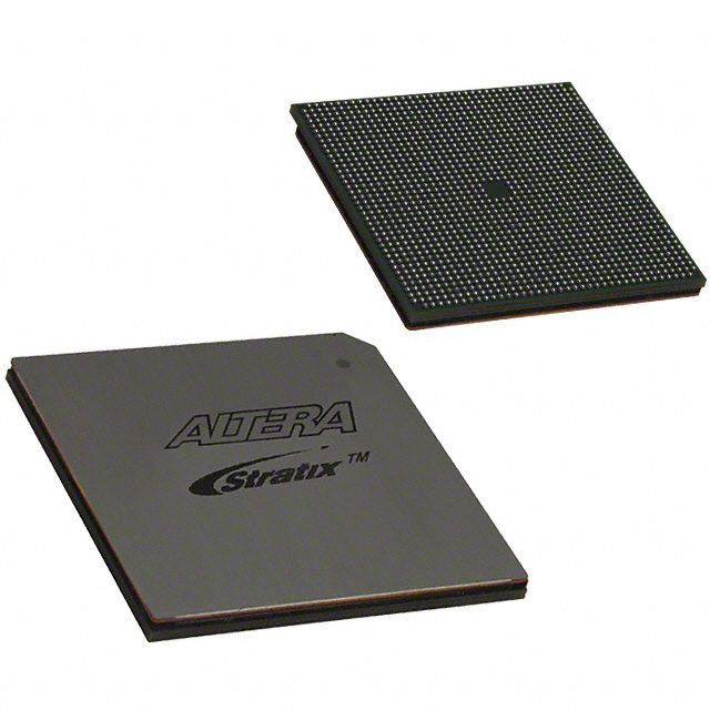
EP2SGX90FF1508C5N
| Part Description |
Stratix® II GX Field Programmable Gate Array (FPGA) IC 650 4520448 90960 1508-BBGA, FCBGA |
|---|---|
| Quantity | 830 Available (as of June 10, 2026) |

| Product Category | Field Programmable Gate Array (FPGA) |
|---|---|
| Manufacturer | Intel |
| Manufacturing Status | Obsolete |
| Manufacturer Standard Lead Time | Contact Us |
| Datasheet |
Specifications & Environmental
| Device Package | 1508-FBGA, FC (40x40) | Grade | Commercial | Operating Temperature | 0°C – 85°C | ||
|---|---|---|---|---|---|---|---|
| Package / Case | 1508-BBGA, FCBGA | Number of I/O | 650 | Voltage | 1.15 V - 1.25 V | ||
| Mounting Method | Surface Mount | RoHS Compliance | RoHS Compliant | REACH Compliance | REACH Unaffected | ||
| Moisture Sensitivity Level | 3 (168 Hours) | Number of LABs/CLBs | 4548 | Number of Logic Elements/Cells | 90960 | ||
| Number of Gates | N/A | ECCN | 3A001A7A | HTS Code | 8542.39.0001 | ||
| Qualification | N/A | Total RAM Bits | 4520448 |
Overview of EP2SGX90FF1508C5N – Stratix® II GX Field Programmable Gate Array (FPGA) IC
The EP2SGX90FF1508C5N is a Stratix® II GX family FPGA from Intel, delivering a high-density, high-performance programmable logic platform. It pairs a large logic array—90,960 logic elements—with substantial embedded memory and extensive I/O to address demanding communications, backplane, and protocol-bridging applications.
Built on the Stratix II GX architecture, this device benefits from family-level high-speed serial transceiver technology and advanced on-chip resources, while offering commercial-grade operation, RoHS compliance, and a compact 1508-ball FCBGA package for high-density system integration.
Key Features
- Logic Capacity Provides 90,960 logic elements for complex programmable logic and system integration.
- Embedded Memory Approximately 4.52 Mbits of on-chip RAM to implement FIFOs, dual-port memories, and buffer structures.
- I/O Density 650 user I/O pins support broad interface requirements and flexible board-level connectivity.
- Stratix II GX Transceiver Capabilities (family) The Stratix II GX family includes high-speed serial transceiver technology with per-channel data rates up to 6.375 Gbps and family-level support for dynamic reconfiguration, adaptive equalization, and programmable pre-emphasis.
- DSP and Clock Resources (family) Family features include high-speed DSP blocks for multipliers and MAC functions (up to 450 MHz) and up to 16 global clock networks with extensive regional clock routing.
- Memory Architecture (family) TriMatrix memory architecture provides multiple RAM block sizes to implement true dual-port memory and high-performance FIFOs with operating performance up to 550 MHz.
- Package & Mounting 1508-ball BGA (FCBGA) package, surface-mount design, supplier package listed as 1508-FBGA, FC (40×40) for compact system integration.
- Power & Supply Core supply operation between 1.15 V and 1.25 V to match Stratix II GX device power requirements.
- Operating Range & Compliance Commercial grade device with an operating temperature range of 0 °C to 85 °C and RoHS compliance for environmental regulation adherence.
Typical Applications
- High-Speed Backplane Interfaces High logic density and family-level transceiver capabilities make this device suitable for backplane protocol bridging and board-to-board communications.
- Chip-to-Chip Connectivity Large I/O counts and high-speed serial support enable flexible chip-to-chip interfacing and custom protocol implementation.
- Network & Telecom Equipment Use the device’s embedded memory, DSP blocks, and Stratix II GX transceiver features for packet processing, framing, and protocol adaptation functions.
- High-Performance Prototyping Substantial logic capacity and memory allow system designers to prototype complex architectures and accelerate time-to-market.
Unique Advantages
- High Integration Density: 90,960 logic elements and approximately 4.52 Mbits of embedded memory reduce external component count and simplify system designs.
- Extensive I/O Resources: 650 I/Os provide the flexibility to support many parallel interfaces and mixed-signal connectivity on a single device.
- Family-Level High-Speed Serial Support: Stratix II GX transceiver technology (up to 6.375 Gbps per channel at the family level) enables implementation of modern serial protocols and high-throughput links.
- Advanced On-Chip DSP & Memory Architecture: Dedicated DSP blocks and TriMatrix memory architecture support high-speed arithmetic and buffering functions required in communications and signal-processing applications.
- Compact, Board-Friendly Package: 1508-ball FCBGA package (40×40) and surface-mount mounting help conserve PCB area while supporting high pin count designs.
- Regulatory and Grade Suitability: Commercial grade operation (0 °C to 85 °C) and RoHS compliance support standard commercial product deployments.
Why Choose EP2SGX90FF1508C5N?
The EP2SGX90FF1508C5N positions itself as a high-density, commercially graded FPGA solution for designers who need significant programmable logic, embedded memory, and broad I/O capability in a compact package. Leveraging the Stratix II GX family architecture delivers access to advanced transceiver technologies and DSP/memory resources that help accelerate development of communications, backplane, and chip-to-chip systems.
This device is well suited for engineering teams aiming to consolidate functions, reduce board-level complexity, and scale solutions within the Stratix II GX ecosystem while maintaining standard commercial operating characteristics and RoHS compliance.
Request a quote or submit an RFQ to obtain pricing, availability, and ordering information for EP2SGX90FF1508C5N. Our team will respond with the details you need to move your design forward.


Date Founded: 1968
Headquarters: Santa Clara, California, USA
Employees: 130,000+
Revenue: $54.23 Billion
Certifications and Memberships: ISO9001:2015, ISO14001:2015, ISO17025:2017, ISO27001:2022, ISO45001:2018, ISO50001:2018


