
EP3CLS150F484C7
| Part Description |
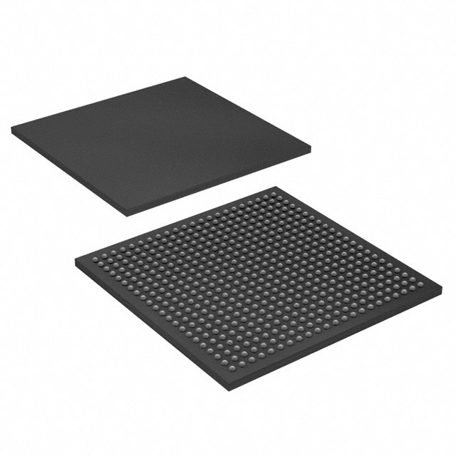
Cyclone® III Field Programmable Gate Array (FPGA) IC 210 6137856 150848 484-BGA |
|---|---|
| Quantity | 1,087 Available (as of June 18, 2026) |

| Product Category | Field Programmable Gate Array (FPGA) |
|---|---|
| Manufacturer | Intel |
| Manufacturing Status | Active |
| Manufacturer Standard Lead Time | 26 Weeks |
| Datasheet |
Specifications & Environmental
| Device Package | 484-FBGA (23x23) | Grade | Commercial | Operating Temperature | 0°C – 85°C | ||
|---|---|---|---|---|---|---|---|
| Package / Case | 484-BGA | Number of I/O | 210 | Voltage | 1.15 V - 1.25 V | ||
| Mounting Method | Surface Mount | RoHS Compliance | RoHS non-compliant | REACH Compliance | REACH Unaffected | ||
| Moisture Sensitivity Level | 3 (168 Hours) | Number of LABs/CLBs | 9428 | Number of Logic Elements/Cells | 150848 | ||
| Number of Gates | N/A | ECCN | 3A991D | HTS Code | 8542.39.0001 | ||
| Qualification | N/A | Total RAM Bits | 6137856 |
Overview of EP3CLS150F484C7 – Cyclone® III Field Programmable Gate Array (FPGA) IC, 150,848 Logic Elements, 484‑BGA
The EP3CLS150F484C7 is a Cyclone III family FPGA offered by Intel, delivering 150,848 logic elements and approximately 6.14 Mbits of embedded memory in a 484‑ball FBGA (23×23) package. With 210 programmable I/O pins and a 1.15 V to 1.25 V core supply range, this commercial‑grade, surface‑mount device targets high‑functionality, low‑power designs.
Designed for cost‑ and power‑sensitive applications, the Cyclone III family combines on‑chip memory, abundant logic, and clock management capabilities to support system integration in compact board layouts while meeting RoHS environmental requirements.
Key Features
- Logic Capacity 150,848 logic elements provide substantial programmable fabric for complex digital functions and custom logic implementation.
- Embedded Memory Approximately 6.14 Mbits of on‑chip RAM to support buffers, FIFOs, and embedded data storage without external memory for many use cases.
- I/O and Interface Density 210 user I/Os available for diverse peripheral and interface requirements, enabling flexible board routing and system connectivity.
- Clock Management Cyclone III family devices include multi‑PLL clock management features for robust clock synthesis and distribution across logic and I/O domains.
- Power and Supply Low core voltage operation (1.15 V to 1.25 V) consistent with low‑power system designs; family optimizations focus on minimizing static power.
- Package and Mounting 484‑FBGA (23×23) surface‑mount package supports compact PCB layouts while providing the I/O density required for mid‑range FPGA applications.
- Operating Range and Grade Commercial grade with an operating temperature range of 0 °C to 85 °C, suitable for typical commercial and consumer environments.
- Environmental Compliance RoHS compliant to meet common environmental and manufacturing requirements.
Typical Applications
- Embedded Control and Processing Use the on‑chip logic and memory to implement control algorithms, state machines, and custom accelerators for appliances, instrumentation, and control systems.
- Communications and Networking High I/O count and flexible clocking make the device suitable for protocol bridging, packet processing, and interface aggregation tasks.
- Consumer and Portable Electronics Low‑power family characteristics and compact FBGA packaging support feature‑rich consumer devices and handheld equipment where energy efficiency matters.
- Prototyping and System Integration Large logic density and embedded memory enable system designers to prototype complex SoC functions and integrate multiple functions onto a single FPGA.
Unique Advantages
- High Logic Density: 150,848 logic elements allow consolidation of multiple functions into one device, reducing board complexity and bill of materials.
- On‑chip Memory Resources: Approximately 6.14 Mbits of embedded RAM minimizes reliance on external memory, improving latency and simplifying PCB design.
- Flexible I/O Count: 210 I/Os accommodate a wide mix of external interfaces without extensive multiplexing, accelerating time to market.
- Compact, Surface‑Mount Package: 484‑FBGA (23×23) enables dense PCB layouts and supports compact system form factors.
- Low Core Voltage Operation: 1.15 V to 1.25 V supply range aligns with low‑power system requirements and helps reduce overall power consumption.
- Proven Family Capabilities: Built on the Cyclone III device family, which emphasizes low power and system integration features such as multi‑PLL clock management and on‑device resources.
Why Choose EP3CLS150F484C7?
The EP3CLS150F484C7 provides a balance of high logic capacity, significant embedded memory, and ample I/O in a compact 484‑FBGA package, making it a strong fit for commercial designs that require integration and power efficiency. Its specification profile supports designers who need to consolidate functions, implement high‑throughput logic, and minimize external components.
Backed by the Cyclone III device family design philosophy, this part is suited for customers pursuing scalable FPGA solutions with robust clocking and memory resources, while maintaining compliance with common environmental standards.
Request a quote or submit a pricing inquiry to evaluate EP3CLS150F484C7 for your next design project.


Date Founded: 1968
Headquarters: Santa Clara, California, USA
Employees: 130,000+
Revenue: $54.23 Billion
Certifications and Memberships: ISO9001:2015, ISO14001:2015, ISO17025:2017, ISO27001:2022, ISO45001:2018, ISO50001:2018


