
EP3SL200F1152C4LN
| Part Description |
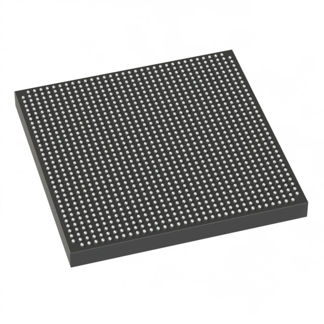
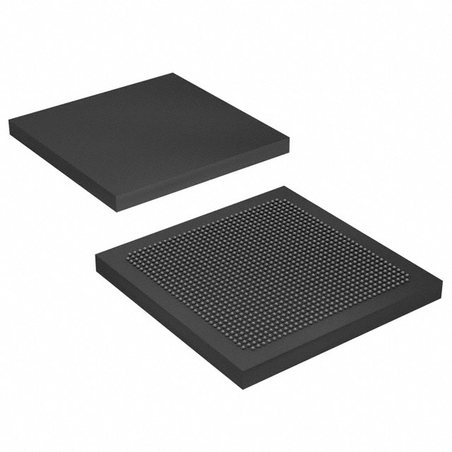
Stratix® III L Field Programmable Gate Array (FPGA) IC 744 10901504 200000 1152-BBGA, FCBGA |
|---|---|
| Quantity | 576 Available (as of June 14, 2026) |

| Product Category | Field Programmable Gate Array (FPGA) |
|---|---|
| Manufacturer | Intel |
| Manufacturing Status | Obsolete |
| Manufacturer Standard Lead Time | Contact Us |
| Datasheet |
Specifications & Environmental
| Device Package | 1152-FBGA (35x35) | Grade | Commercial | Operating Temperature | 0°C – 85°C | ||
|---|---|---|---|---|---|---|---|
| Package / Case | 1152-BBGA, FCBGA | Number of I/O | 744 | Voltage | 860 mV - 1.15 V | ||
| Mounting Method | Surface Mount | RoHS Compliance | RoHS Compliant | REACH Compliance | REACH Unknown | ||
| Moisture Sensitivity Level | 3 (168 Hours) | Number of LABs/CLBs | 8000 | Number of Logic Elements/Cells | 200000 | ||
| Number of Gates | N/A | ECCN | 3A001A2C | HTS Code | 8542.39.0001 | ||
| Qualification | N/A | Total RAM Bits | 10901504 |
Overview of EP3SL200F1152C4LN – Stratix® III L FPGA, 200,000 Logic Elements
The EP3SL200F1152C4LN is a Stratix® III L field-programmable gate array (FPGA) from Intel offering high logic density and a large on-chip memory budget in a compact FCBGA package. It targets designs that require substantial programmable logic capacity, extensive I/O, and low-voltage core operation.
Key value propositions include 200,000 logic elements, approximately 10.9 Mbits of embedded memory, and 744 I/O pins—all delivered in a 1152-FBGA (35×35) / 1152-BBGA surface-mount package with commercial-grade temperature and RoHS compliance.
Key Features
- Core Logic 200,000 logic elements provide high-density programmable logic for complex digital designs.
- Embedded Memory Approximately 10.9 Mbits of on-chip RAM for buffering, temporary storage, and local data processing.
- I/O Capacity 744 general-purpose I/O pins to support wide parallel interfaces and high pin-count connectivity.
- Power and Supply Low-voltage core operation supported across a supply range of 0.86 V to 1.15 V to match platform power requirements.
- Package and Mounting Available in a 1152-FBGA (35×35) / 1152-BBGA (FCBGA) surface-mount package to optimize board density and thermal pathing.
- Temperature and Grade Commercial operating range of 0 °C to 85 °C for typical commercial and industrial-adjacent applications.
- Regulatory RoHS compliant for environmental and manufacturing compatibility.
Typical Applications
- High-density digital systems — Leverages 200,000 logic elements and substantial embedded memory to implement large combinational and sequential logic networks.
- I/O-intensive interfaces — The 744 I/O pins enable integration of multiple parallel buses, wide data paths, or numerous sensor and peripheral connections.
- On-board buffering and local storage — Approximately 10.9 Mbits of embedded RAM supports packet buffering, FIFOs, and temporary data storage close to logic elements.
- Compact platform designs — The 1152-FBGA (35×35) surface-mount package helps reduce PCB footprint while maintaining high connectivity.
Unique Advantages
- High logic capacity: 200,000 logic elements enable integration of complex functionality on a single device, reducing the need for multi-chip solutions.
- Significant on-chip memory: Approximately 10.9 Mbits of embedded RAM minimizes external memory dependence for many buffering and data-path needs.
- Extensive I/O support: 744 I/O pins provide flexibility for wide interfaces and numerous peripherals without additional I/O expander components.
- Compact FCBGA packaging: 1152-FBGA (35×35) / 1152-BBGA surface-mount package conserves board area while supporting high pin counts.
- Low-voltage core: 0.86–1.15 V supply range accommodates low-voltage system architectures.
- RoHS compliant: Meets environmental and manufacturing requirements for lead-free assembly.
Why Choose EP3SL200F1152C4LN?
Manufactured by Intel, the EP3SL200F1152C4LN combines very high logic density, large embedded memory, and an extensive I/O complement in a compact surface-mount FCBGA package. It is well suited for designers who need to consolidate complex logic, substantial on-chip RAM, and broad connectivity into a single FPGA device for commercial-temperature applications.
For projects requiring a commercially graded FPGA with high integration and a low-voltage core profile, this device provides a clear balance of capacity, I/O, and packaging to support scalable, space-efficient designs.
If you would like pricing or availability details, request a quote or submit a purchase inquiry and our team will respond with the information you need.


Date Founded: 1968
Headquarters: Santa Clara, California, USA
Employees: 130,000+
Revenue: $54.23 Billion
Certifications and Memberships: ISO9001:2015, ISO14001:2015, ISO17025:2017, ISO27001:2022, ISO45001:2018, ISO50001:2018


