
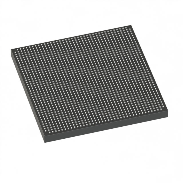
EP3SL200F1517C2
| Part Description |
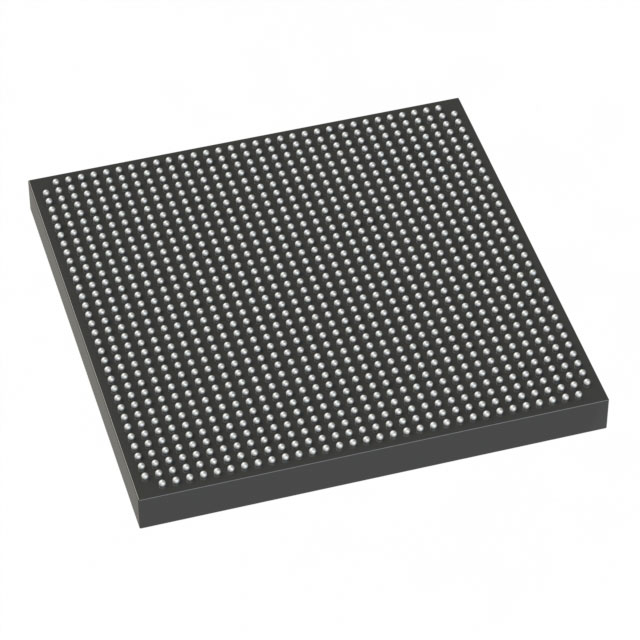
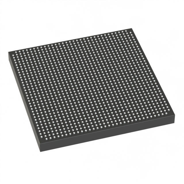
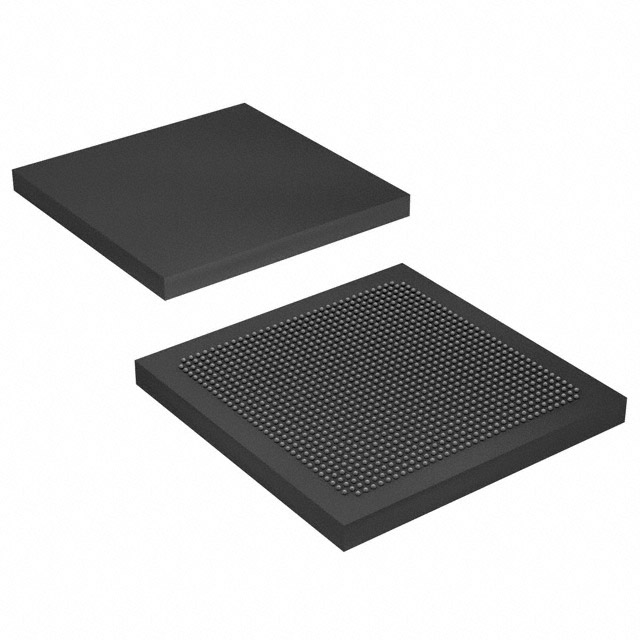
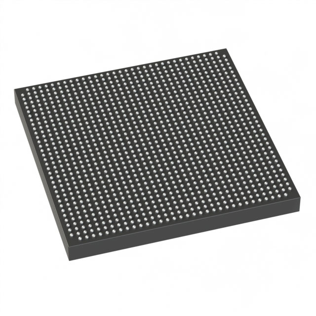
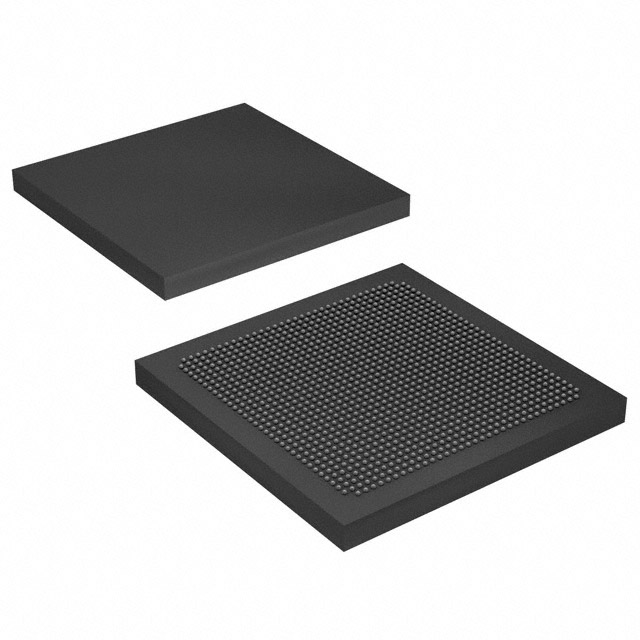
Stratix® III L Field Programmable Gate Array (FPGA) IC 976 10901504 200000 1517-BBGA, FCBGA |
|---|---|
| Quantity | 31 Available (as of October 7, 2026) |
| Product Category | Field Programmable Gate Array (FPGA) |
|---|---|
| Manufacturer | Intel |
| Manufacturing Status | Obsolete |
| Manufacturer Standard Lead Time | Contact Us |
| Datasheet |
Specifications & Environmental
| Device Package | 1517-FBGA (40x40) | Grade | Commercial | Operating Temperature | 0°C – 85°C | ||
|---|---|---|---|---|---|---|---|
| Package / Case | 1517-BBGA, FCBGA | Number of I/O | 976 | Voltage | 860 mV - 1.15 V | ||
| Mounting Method | Surface Mount | RoHS Compliance | RoHS Compliant | REACH Compliance | REACH Unknown | ||
| Moisture Sensitivity Level | 3 (168 Hours) | Number of LABs/CLBs | 8000 | Number of Logic Elements/Cells | 200000 | ||
| Number of Gates | N/A | ECCN | 3A001A2C | HTS Code | 8542.39.0001 | ||
| Qualification | N/A | Total RAM Bits | 10901504 |
Overview of EP3SL200F1517C2 – Stratix® III L FPGA, 200,000 logic elements, 976 I/Os
The EP3SL200F1517C2 is a Stratix® III L Field Programmable Gate Array (FPGA) offering high logic density and extensive I/O in a compact FCBGA package. With 200,000 logic elements and approximately 10.9 Mbits of embedded memory, it is aimed at commercial designs that require large on‑chip logic and memory capacity.
Its feature set—including 976 I/Os, a 1517‑FBGA (40×40) footprint, and a supply voltage range of 0.86 V to 1.15 V—makes it suitable for I/O‑intensive and high‑density digital applications operating in commercial temperature environments (0 °C to 85 °C).
Key Features
- Core Logic Capacity 200,000 logic elements provide substantial programmable logic resources for complex digital designs.
- Embedded Memory Approximately 10.9 Mbits of on‑chip RAM to support buffers, FIFOs, and local data storage for processing pipelines.
- I/O Density 976 user I/Os enable broad external interfacing for high‑channel count designs or dense connector requirements.
- Power and Voltage Operates across a supply voltage range of 0.86 V to 1.15 V to match system power architectures.
- Package and Mounting Delivered in a 1517‑BBGA (FCBGA) package — supplier device package listed as 1517‑FBGA (40×40) — for surface‑mount assembly.
- Operating Range Commercial grade operation from 0 °C to 85 °C for standard commercial applications.
- Environmental Compliance RoHS compliant to meet common industry environmental requirements.
Typical Applications
- Telecommunications and Networking High logic and I/O counts support packet processing, protocol bridging, and custom interface implementations.
- Data Acquisition and Signal Processing Large on‑chip RAM and dense logic resources enable buffering and real‑time processing of multi‑channel data streams.
- FPGA Prototyping and System Integration Suitable for prototyping complex digital systems that require significant programmable logic and external connectivity.
- Test and Measurement Equipment Provides the capacity for custom control logic and data handling in commercial test systems.
Unique Advantages
- High Logic Capacity: 200,000 logic elements allow implementation of large, complex designs without immediate need for multiple devices.
- Substantial On‑Chip Memory: Approximately 10.9 Mbits of embedded RAM reduces reliance on external memory for many buffering and processing tasks.
- Extensive External Connectivity: 976 I/Os enable flexible interfacing to peripherals, sensors, transceivers, and board‑level interconnects.
- Compact FCBGA Footprint: 1517‑FBGA (40×40) package optimizes board space while supporting surface‑mount assembly processes.
- Commercial Temperature Range: Rated 0 °C to 85 °C for reliable operation in standard commercial environments.
- RoHS Compliant: Meets environmental compliance expectations for modern electronics manufacturing.
Why Choose EP3SL200F1517C2?
The EP3SL200F1517C2 delivers a combination of high logic density, sizable embedded memory, and broad I/O capability in a compact FCBGA package—attributes that align with demanding commercial designs requiring on‑chip integration of complex digital functions. As a member of the Stratix® III L family from Intel, it provides designers with the resources needed to implement large-scale logic, buffering, and multi‑channel interfacing within a single device.
This part is well suited to engineering teams developing telecommunications, data acquisition, and prototype systems where on‑chip resources and I/O density reduce board complexity and BOM count while operating within a standard commercial temperature range.
Request a quote or submit a pricing inquiry to get availability and lead‑time information for EP3SL200F1517C2.





















Date Founded: 1968
Headquarters: Santa Clara, California, USA
Employees: 130,000+
Revenue: $54.23 Billion
Certifications and Memberships: ISO9001:2015, ISO14001:2015, ISO17025:2017, ISO27001:2022, ISO45001:2018, ISO50001:2018


