
EP3SL200F1517C2G
| Part Description |
Field Programmable Gate Array (FPGA) IC |
|---|---|
| Quantity | 469 Available (as of June 15, 2026) |

| Product Category | Field Programmable Gate Array (FPGA) |
|---|---|
| Manufacturer | Intel |
| Manufacturing Status | Active |
| Manufacturer Standard Lead Time | 26 Weeks |
| Datasheet |
Specifications & Environmental
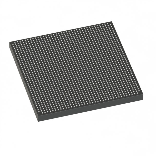
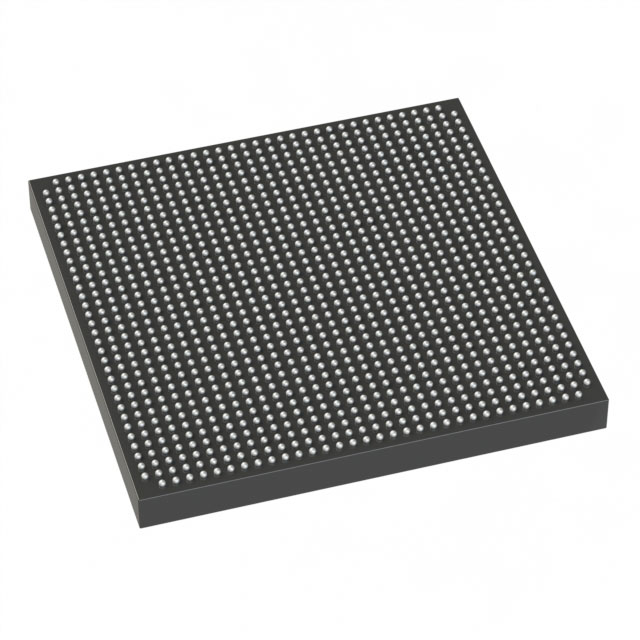
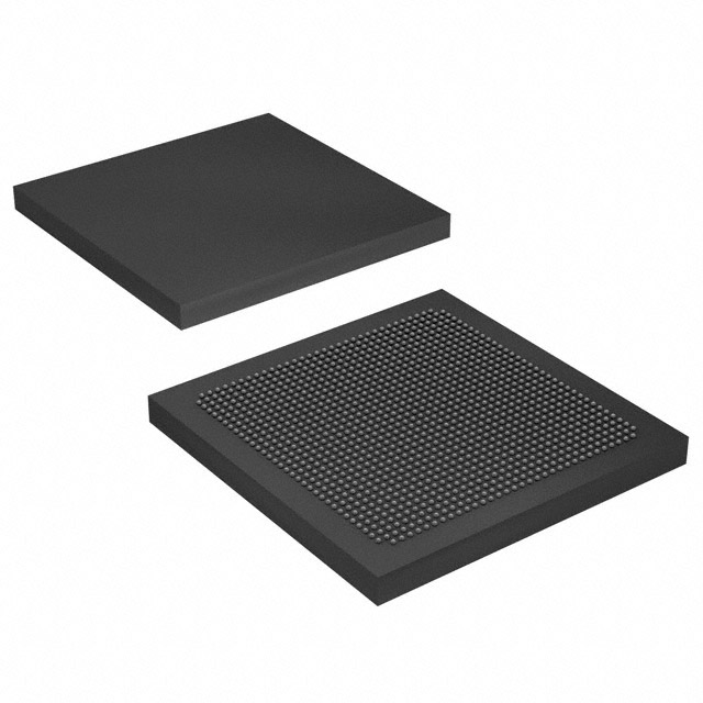
| Device Package | 1517-FBGA (40x40) | Grade | Commercial | Operating Temperature | 0°C – 85°C | ||
|---|---|---|---|---|---|---|---|
| Package / Case | 1517-BBGA, FCBGA | Number of I/O | 976 | Voltage | 860 mV - 1.15 V | ||
| Mounting Method | Surface Mount | RoHS Compliance | RoHS Compliant | REACH Compliance | REACH Unaffected | ||
| Moisture Sensitivity Level | 3 (168 Hours) | Number of LABs/CLBs | 8000 | Number of Logic Elements/Cells | 200000 | ||
| Number of Gates | N/A | ECCN | N/A | HTS Code | N/A | ||
| Qualification | N/A | Total RAM Bits | 10901504 |
Overview of EP3SL200F1517C2G – Field Programmable Gate Array (FPGA) IC
The EP3SL200F1517C2G is a Stratix III family FPGA delivering a high-density, configurable logic platform for performance-focused embedded and digital signal processing applications. Built on a 65 nm, 1.1 V SRAM process with selectable core voltage support, this device combines large logic capacity, substantial embedded memory, and extensive I/O to support complex system integration and high-speed interfaces.
Targeted at commercial applications, the device is optimized for designs that require large logic resources, significant on-chip memory, and flexible I/O routing while operating within a 0 °C to 85 °C range and a core supply range of 0.860 V to 1.150 V.
Key Features
- Logic Capacity Approximately 200,000 logic elements for implementing dense combinational and sequential logic, custom data paths, and state machines.
- Embedded Memory Approximately 10.9 Mbits of on-chip RAM (10,901,504 bits) for FIFOs, buffers, and storage of intermediate data.
- I/O and Package Up to 976 user I/O pins in a 1517-FBGA (40×40) FCBGA package with surface-mount mounting for high-density board designs.
- Core Voltage Range Configurable core supply from 0.860 V to 1.150 V to balance performance and power for different system needs.
- Clocking and PLLs Rich clocking architecture with up to 16 global clocks, numerous regional and peripheral clocks, and support for up to 12 phase-locked loops for complex timing domains and clock synthesis.
- DSP and Arithmetic Support Architecture includes high-speed DSP/multiplier resources suitable for dedicated multiply-accumulate and signal-processing functions.
- Memory Interface and Signal Integrity Family features include dedicated memory interface support and dynamic on-chip termination and calibration for robust high-speed signaling.
- System Reliability and Security Configuration CRC and optional AES-based configuration security and ECC protection for on-chip memory blocks as part of family-level features.
- Compliance RoHS compliant and supplied in a commercial-grade package rated for 0 °C to 85 °C operation.
Typical Applications
- High-performance DSP systems Implement FIR filters, matrix operations, and real-time signal processing using the device’s DSP resources and large logic fabric.
- Embedded compute and control Integrate soft processors, custom accelerators, and control logic for communications equipment and industrial controllers within the commercial temperature range.
- Memory interface controllers Use the device’s embedded memory and memory-interface support to implement DDR/DDR2/DDR3 or other high-speed memory front-ends and buffering.
- High-density I/O and protocol bridging Leverage up to 976 I/Os and modular I/O bank structure to implement multi-protocol bridging, protocol aggregation, and complex interface routing.
Unique Advantages
- High logic density: The substantial logic element count enables complex logic consolidation and reduces the need for multiple devices on a board.
- Large on-chip memory: Approximately 10.9 Mbits of embedded RAM simplifies buffer and FIFO designs and reduces external memory dependence.
- Flexible I/O and package options: 976 user I/Os in a 1517-FBGA (40×40) package provide ample connectivity for high-pin-count designs while supporting surface-mount assembly.
- Configurable power/performance: Core voltage range from 0.860 V to 1.150 V enables design trade-offs between performance and power consumption.
- Robust clocking and PLL resources: Multiple clock domains and up to 12 PLLs support complex timing architectures and high-speed clock synthesis.
- Family-level reliability and security: Built-in CRC, ECC for memory blocks, and optional AES configuration security help protect configuration and system data.
Why Choose EP3SL200F1517C2G?
The EP3SL200F1517C2G balances high logic capacity, substantial embedded memory, and a wide complement of I/O in a commercial-grade Stratix III FPGA package. It is suited to engineers designing demanding DSP, embedded compute, and high-speed interface systems who need a programmable, high-density platform with flexible power and clocking options.
With family-level features for memory interface support, on-chip termination, configurable clocking, and security, this device offers a scalable foundation for systems that require integration of logic, memory, and high-speed I/O while maintaining design flexibility.
Request a quote or submit an inquiry to receive pricing and availability information for the EP3SL200F1517C2G and to discuss how it fits your next design.


Date Founded: 1968
Headquarters: Santa Clara, California, USA
Employees: 130,000+
Revenue: $54.23 Billion
Certifications and Memberships: ISO9001:2015, ISO14001:2015, ISO17025:2017, ISO27001:2022, ISO45001:2018, ISO50001:2018


