
EP3SL200F1517C3G
| Part Description |
Field Programmable Gate Array (FPGA) IC |
|---|---|
| Quantity | 1,258 Available (as of June 10, 2026) |

| Product Category | Field Programmable Gate Array (FPGA) |
|---|---|
| Manufacturer | Intel |
| Manufacturing Status | Active |
| Manufacturer Standard Lead Time | 26 Weeks |
| Datasheet |
Specifications & Environmental
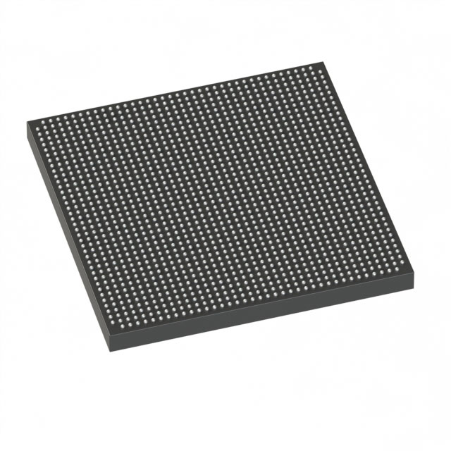
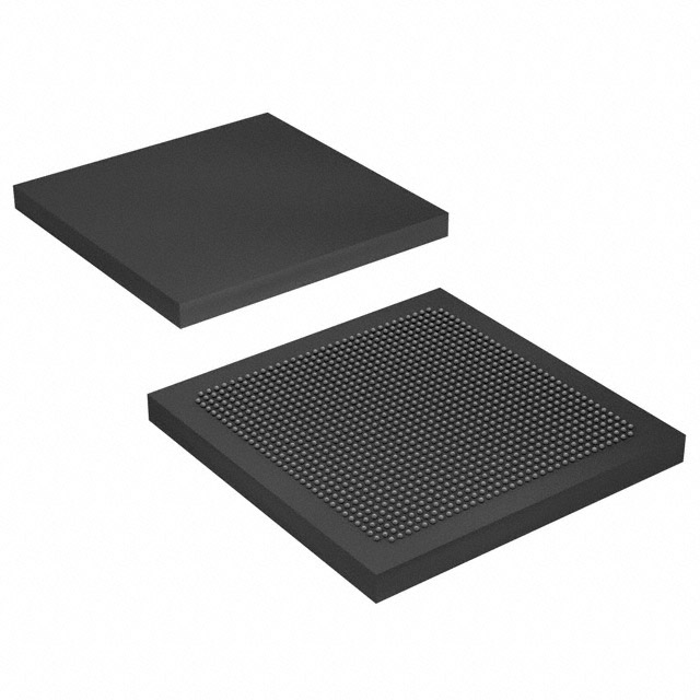
| Device Package | 1517-FBGA (40x40) | Grade | Commercial | Operating Temperature | 0°C – 85°C | ||
|---|---|---|---|---|---|---|---|
| Package / Case | 1517-BBGA, FCBGA | Number of I/O | 976 | Voltage | 860 mV - 1.15 V | ||
| Mounting Method | Surface Mount | RoHS Compliance | RoHS Compliant | REACH Compliance | REACH Unaffected | ||
| Moisture Sensitivity Level | 3 (168 Hours) | Number of LABs/CLBs | 8000 | Number of Logic Elements/Cells | 200000 | ||
| Number of Gates | N/A | ECCN | N/A | HTS Code | N/A | ||
| Qualification | N/A | Total RAM Bits | 10901504 |
Overview of EP3SL200F1517C3G – Field Programmable Gate Array (FPGA) IC
The EP3SL200F1517C3G is an Intel Stratix III family FPGA offering high-density programmable logic and on-chip memory for demanding digital designs. It combines 200,000 logic elements with approximately 10.9 Mbits of embedded RAM and extensive I/O to support high-performance signal processing, memory interfaces, and system integration.
Designed for commercial applications, this surface-mount FCBGA device provides selectable core voltage operation, advanced DSP support, and platform-level features for reliable configuration and runtime operation.
Key Features
- Logic Capacity — 200,000 logic elements to implement complex custom logic, control functions, and large-scale state machines.
- Embedded Memory — Approximately 10.9 Mbits of on-chip RAM for buffering, FIFOs, and on-chip data storage.
- I/O Density — 976 user I/O pins arranged for modular I/O bank architectures to support diverse interface standards and external memory connections.
- DSP and Arithmetic — High-speed DSP block support with dedicated multipliers (including 9×9, 12×12, 18×18, and 36×36 multiplier options) for hardware-accelerated signal processing and multiply-accumulate tasks.
- Clocking Resources — On-chip clocking and PLL resources (family-level support includes multiple global, regional, and peripheral clocks and up to 12 PLLs) to enable complex timing domains and clock synthesis.
- High-Speed I/O Support — Differential I/O and SERDES/DPA circuitry for high-speed serial links (family-level support for 1.6 Gbps signaling and dynamic phase alignment), enabling networking and high-throughput interfaces.
- Power and Voltage — Core supply range from 0.86 V to 1.15 V to support selectable core voltage operation for performance vs. power trade-offs.
- Package and Mounting — 1517-BBGA (FCBGA) package, supplier package 1517-FBGA (40×40), surface-mount mounting suitable for dense board-level integration.
- Operating Conditions — Commercial-grade device rated for 0°C to 85°C ambient operating temperature.
- Security & Reliability — Stratix III family-level features include optional 256-bit AES configuration encryption, CRC-based configuration memory checks, and built-in ECC for TriMatrix memory blocks to support robust system operation.
- Standards & Compliance — RoHS compliant.
Typical Applications
- High-Performance Networking — Use the device’s DSP blocks, SERDES support, and large logic capacity to implement packet processing, switching fabrics, and custom networking accelerators.
- Memory Interface Controllers — Implement DDR/DDR2/DDR3 and other high-speed memory controllers leveraging the device’s modular I/O banks and dedicated DQS logic support at the family level.
- Signal Processing and Acceleration — Deploy dedicated multipliers and embedded RAM for FIR filters, FFTs, and real-time DSP pipelines in communications and instrumentation systems.
- Custom Compute and Control — Integrate complex control logic, state machines, and embedded soft processors for industrial automation, test equipment, and prototype ASIC replacement in commercial designs.
Unique Advantages
- High Logic Density: 200,000 logic elements enable large, integrated designs that reduce partitioning across multiple devices.
- Substantial On-Chip Memory: Approximately 10.9 Mbits of embedded RAM lowers external memory dependence and improves latency for buffering and on-chip data processing.
- Flexible I/O and High-Speed Links: 976 user I/O pins and family-level SERDES support provide the flexibility to connect to a wide range of peripherals and high-speed buses.
- Dedicated DSP Resources: Multiple multiplier sizes and DSP blocks accelerate compute-heavy tasks and simplify implementation of signal-processing algorithms.
- Configurable Power Envelope: Core voltage range of 0.86 V–1.15 V lets designers tune for performance or lower power operation within the commercial temperature range.
- Reliability Features: Family-level AES configuration options, CRC checks, and ECC memory protection enhance design security and runtime integrity.
Why Choose EP3SL200F1517C3G?
The EP3SL200F1517C3G brings substantial logic capacity, abundant embedded memory, and extensive I/O resources in a single FCBGA package aimed at commercial applications that require high integration and configurable performance. Its combination of DSP resources, clocking flexibility, and family-level reliability features makes it well suited for networking, memory interface, and signal-processing designs where on-chip acceleration and tight system integration matter.
For design teams targeting scalable, FPGA-based solutions, this device offers a balance of compute, memory, and I/O that supports complex algorithms and high-throughput data paths while maintaining commercial-grade operating conditions and RoHS compliance.
Request a quote or submit a purchase inquiry to get pricing and availability for EP3SL200F1517C3G.


Date Founded: 1968
Headquarters: Santa Clara, California, USA
Employees: 130,000+
Revenue: $54.23 Billion
Certifications and Memberships: ISO9001:2015, ISO14001:2015, ISO17025:2017, ISO27001:2022, ISO45001:2018, ISO50001:2018


