
EP3SL200F1517C3N
| Part Description |
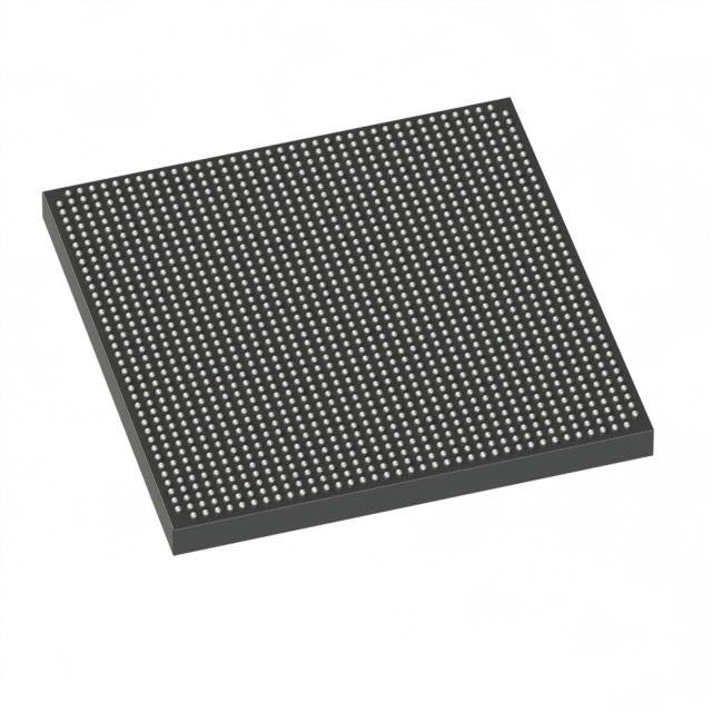
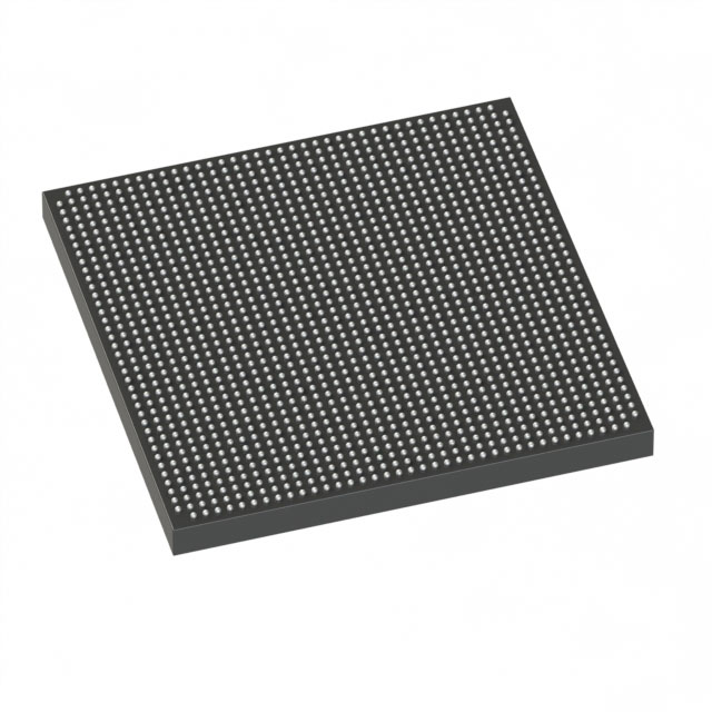
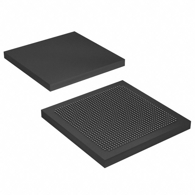
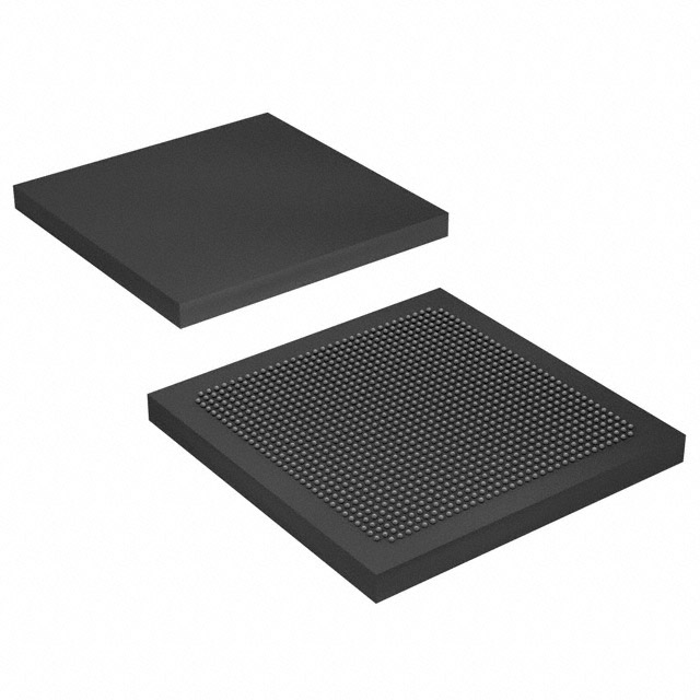
Stratix® III L Field Programmable Gate Array (FPGA) IC 976 10901504 200000 1517-BBGA, FCBGA |
|---|---|
| Quantity | 57 Available (as of October 8, 2026) |
| Product Category | Field Programmable Gate Array (FPGA) |
|---|---|
| Manufacturer | Intel |
| Manufacturing Status | Obsolete |
| Manufacturer Standard Lead Time | Contact Us |
| Datasheet |
Specifications & Environmental
| Device Package | 1517-FBGA (40x40) | Grade | Commercial | Operating Temperature | 0°C – 85°C | ||
|---|---|---|---|---|---|---|---|
| Package / Case | 1517-BBGA, FCBGA | Number of I/O | 976 | Voltage | 860 mV - 1.15 V | ||
| Mounting Method | Surface Mount | RoHS Compliance | RoHS Compliant | REACH Compliance | REACH Unknown | ||
| Moisture Sensitivity Level | 3 (168 Hours) | Number of LABs/CLBs | 8000 | Number of Logic Elements/Cells | 200000 | ||
| Number of Gates | N/A | ECCN | 3A001A7A | HTS Code | 8542.39.0001 | ||
| Qualification | N/A | Total RAM Bits | 10901504 |
Overview of EP3SL200F1517C3N – Stratix III L FPGA, 1517-BBGA
The EP3SL200F1517C3N is a Stratix® III L Field Programmable Gate Array (FPGA) from Intel, offered in a 1517-BBGA FCBGA package. It delivers high logic density, substantial on-chip memory, and a large I/O complement for complex, programmable system designs.
Targeted at commercial-grade applications, this device is well suited for designs requiring dense logic resources, extensive I/O, and embedded memory while operating within a 0 °C to 85 °C temperature range and a core supply of 0.86 V to 1.15 V.
Key Features
- Logic Capacity — Approximately 200,000 logic elements to implement complex digital functions and large-scale programmable logic designs.
- Embedded Memory — Approximately 10.9 Mbits of on-chip RAM to support buffering, data storage, and high-throughput data paths without relying exclusively on external memory.
- High I/O Count — 976 I/O pins to support wide bus interfaces, multi-channel connectivity, and dense external peripheral integration.
- Stratix III Architecture — Family-level architecture details documented in the Stratix III Device Handbook, including multi-track interconnect, TriMatrix embedded memory blocks, DSP blocks, clock networks, and PLLs.
- High-Speed Interfaces — Series documentation references high-speed differential I/O interfaces with DPA and external memory interface support for demanding data applications.
- Configuration & Testability — Device-level features include standard configuration mechanisms and IEEE 1149.1 (JTAG) boundary-scan testing as part of the Stratix III device family documentation.
- Power and Operating Range — Core supply range from 0.86 V to 1.15 V and commercial operating temperature range of 0 °C to 85 °C; surface-mount package (1517-FBGA, 40×40) for compact board-level integration.
- Compliance — RoHS-compliant construction suitable for environmentally regulated assemblies.
Typical Applications
- High-throughput signal processing — Leverage the device's large logic capacity and embedded memory for DSP tasks and streaming data pipelines.
- External memory interfacing — Use the device's architecture and high I/O count to implement memory controllers and wide external memory interfaces.
- Protocol bridging and I/O aggregation — The extensive I/O complement supports protocol conversion, bus aggregation, and multi-channel data routing.
- Custom compute and control — Implement custom control logic, state machines, and application-specific accelerators using the Stratix III resources.
Unique Advantages
- High logic density: Approximately 200,000 logic elements enable the implementation of complex, large-scale designs on a single device.
- Substantial embedded memory: Approximately 10.9 Mbits of on-chip RAM reduce dependency on external memory for buffering and storage.
- Extensive I/O: 976 I/O pins provide flexibility for wide data buses, many peripherals, and multi-channel interfaces.
- Family-level architecture: Stratix III device architecture (documented in the Stratix III Device Handbook) provides integrated building blocks such as DSP and memory primitives for system designers.
- Compact, surface-mount package: 1517-BBGA (1517-FBGA, 40×40) package supports high-density board layouts while maintaining required pin count.
- Commercial-grade readiness: Rated for 0 °C to 85 °C and RoHS compliance for commercial applications and regulated assemblies.
Why Choose EP3SL200F1517C3N?
The EP3SL200F1517C3N combines a high count of logic elements, significant embedded memory, and nearly 1,000 I/O pins in a compact 1517-BBGA package, making it suitable for demanding commercial applications that require on-chip resources and flexible interfacing. As part of the Stratix III family, it benefits from comprehensive device documentation and architecture features that support complex system implementations.
This device is appropriate for teams designing high-throughput signal processing, memory-intensive controllers, or dense interface aggregation solutions who require a commercially rated FPGA backed by the Stratix III device handbook and platform documentation.
Request a quote to check availability and pricing, or submit a quote request to discuss how EP3SL200F1517C3N fits your next design.





















Date Founded: 1968
Headquarters: Santa Clara, California, USA
Employees: 130,000+
Revenue: $54.23 Billion
Certifications and Memberships: ISO9001:2015, ISO14001:2015, ISO17025:2017, ISO27001:2022, ISO45001:2018, ISO50001:2018


