
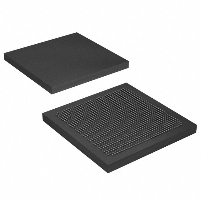
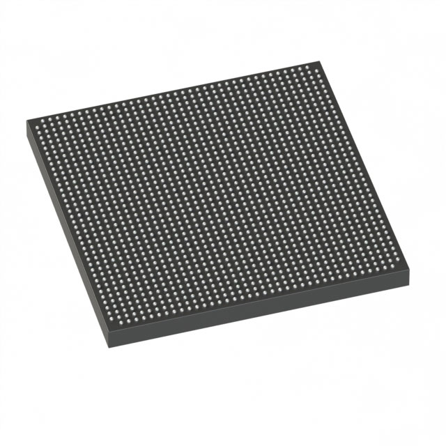
EP3SL200F1517C4LG
| Part Description |
Field Programmable Gate Array (FPGA) IC |
|---|---|
| Quantity | 719 Available (as of June 18, 2026) |
| Product Category | Field Programmable Gate Array (FPGA) |
|---|---|
| Manufacturer | Intel |
| Manufacturing Status | Active |
| Manufacturer Standard Lead Time | 26 Weeks |
| Datasheet |
Specifications & Environmental
| Device Package | 1517-FBGA (40x40) | Grade | Commercial | Operating Temperature | 0°C – 85°C | ||
|---|---|---|---|---|---|---|---|
| Package / Case | 1517-BBGA, FCBGA | Number of I/O | 976 | Voltage | 860 mV - 1.15 V | ||
| Mounting Method | Surface Mount | RoHS Compliance | RoHS Compliant | REACH Compliance | REACH Unaffected | ||
| Moisture Sensitivity Level | 3 (168 Hours) | Number of LABs/CLBs | 8000 | Number of Logic Elements/Cells | 200000 | ||
| Number of Gates | N/A | ECCN | N/A | HTS Code | N/A | ||
| Qualification | N/A | Total RAM Bits | 10901504 |
Overview of EP3SL200F1517C4LG – Field Programmable Gate Array (FPGA) IC
The EP3SL200F1517C4LG is a high-density Field Programmable Gate Array from Intel, implemented on the Stratix III device family architecture. It delivers a combination of large logic capacity, substantial embedded memory, and an extensive I/O complement suitable for demanding logic, DSP and embedded system designs.
Designed for commercial-grade applications, this surface-mount FCBGA device offers selectable core voltage operation and architecture-level power management to balance performance and efficiency in complex multi-function systems.
Key Features
- Core and Logic Approximately 200,000 logic elements provide the programmable fabric for high-density logic and system integration.
- Embedded Memory Approximately 10.9 Mbits of on-chip RAM (10,901,504 total RAM bits) for large buffers, FIFOs and packet/stream processing tasks.
- DSP and Arithmetic Blocks Family-level high-speed DSP blocks support a range of multiplier sizes and multiply-accumulate implementations suitable for signal processing workloads.
- I/O Capacity 976 user I/O pins in a modular I/O bank structure to support wide parallel interfaces and multiple external memory or peripheral connections.
- Clocking and PLLs Multiple on-chip clock resources and PLLs provide flexible clock management for complex timing domains and high-performance designs.
- Power and Core Voltage Selectable core voltage operation with a supply range of 0.86 V to 1.15 V and architecture-level programmable power technology to manage performance versus power.
- Security and Reliability Family-level features include support for 256-bit AES configuration encryption and built-in CRC/ECC mechanisms for configuration and memory integrity.
- Package and Mounting Available in a 1517-FBGA (1517-BBGA, FCBGA) package (40 × 40 mm) for surface-mount board implementation; RoHS compliant.
- Commercial Temperature Rating Specified for operation from 0 °C to 85 °C to meet commercial application requirements.
Typical Applications
- High-Performance Logic and Compute Implement complex control, glue-logic, and acceleration functions where a large count of logic elements and on-chip RAM are required.
- Digital Signal Processing (DSP) Use the device’s DSP-capable fabric and embedded memory for filtering, transforms, and real-time signal processing pipelines.
- Memory Interface and Buffering Leverage the substantial on-chip RAM and abundant I/O for external memory interfacing, buffering and high-throughput data paths.
- Networking and Communications Deploy in systems requiring flexible I/O and clocking to implement protocol bridges, data-path processing, or interface adaptation.
Unique Advantages
- High logic density: Approximately 200,000 logic elements enable consolidation of multiple system functions into a single device, reducing board complexity.
- Large embedded memory: Approximately 10.9 Mbits of on-chip RAM supports sizable FIFOs, packet buffers and state storage without immediate need for external memory.
- Extensive I/O resources: 976 user I/O pins in a modular bank layout give designers the flexibility to connect wide buses and multiple peripherals.
- Configurable power/performance: Selectable core voltage (0.86 V–1.15 V) and programmable power management enable tuning for either higher performance or reduced power consumption.
- Built-in security and integrity: Support for 256-bit AES configuration encryption plus CRC and ECC mechanisms helps protect configuration and on-chip memory integrity.
- Commercial-grade, surface-mount form factor: 1517-FBGA package provides a compact, solderable footprint for production PCBs while meeting commercial operating temperature requirements.
Why Choose EP3SL200F1517C4LG?
The EP3SL200F1517C4LG combines high logic capacity, substantial embedded memory and a broad I/O complement within the Stratix III family architecture to address complex logic, DSP and embedded applications. Its selectable core voltage and family-level programmable power features allow engineers to tune the device for target performance or power budgets.
This part is suited to design teams needing a scalable, commercially-rated FPGA with strong on-chip memory and connectivity for data-path intensive development. The integrated security and integrity features add design robustness for long-term deployments backed by the Stratix III device family documentation and tooling.
Request a quote or submit a purchasing inquiry to evaluate EP3SL200F1517C4LG for your next design.


Date Founded: 1968
Headquarters: Santa Clara, California, USA
Employees: 130,000+
Revenue: $54.23 Billion
Certifications and Memberships: ISO9001:2015, ISO14001:2015, ISO17025:2017, ISO27001:2022, ISO45001:2018, ISO50001:2018


