
EP4SE360F35I4
| Part Description |
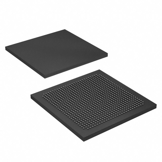
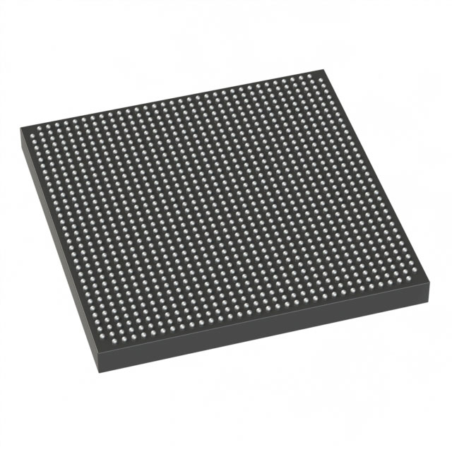
STRATIX® IV E Field Programmable Gate Array (FPGA) IC 744 23105536 353600 1152-BBGA, FCBGA |
|---|---|
| Quantity | 1,132 Available (as of June 15, 2026) |

| Product Category | Field Programmable Gate Array (FPGA) |
|---|---|
| Manufacturer | Intel |
| Manufacturing Status | Obsolete |
| Manufacturer Standard Lead Time | Contact Us |
| Datasheet |
Specifications & Environmental
| Device Package | 1152-FBGA (35x35) | Grade | Industrial | Operating Temperature | -40°C – 100°C | ||
|---|---|---|---|---|---|---|---|
| Package / Case | 1152-BBGA, FCBGA | Number of I/O | 744 | Voltage | 870 mV - 930 mV | ||
| Mounting Method | Surface Mount | RoHS Compliance | RoHS non-compliant | REACH Compliance | REACH Unknown | ||
| Moisture Sensitivity Level | 3 (168 Hours) | Number of LABs/CLBs | 14144 | Number of Logic Elements/Cells | 353600 | ||
| Number of Gates | N/A | ECCN | 3A001A7A | HTS Code | 8542.39.0001 | ||
| Qualification | N/A | Total RAM Bits | 23105536 |
Overview of EP4SE360F35I4 – STRATIX® IV E FPGA, 353,600 logic elements, 744 I/Os
The EP4SE360F35I4 is an Intel STRATIX® IV E field programmable gate array (FPGA) offered in a 1152-ball FCBGA package. It provides a high-density programmable fabric with 353,600 logic elements and approximately 23.1 Mbits of embedded memory, designed for demanding, I/O-rich industrial applications.
Key characteristics visible in the device documentation include high-capacity logic and memory, on-chip DSP and TriMatrix memory block support, documented PLL and clock-tree resources, and dedicated transceiver performance specifications—enabling complex system integration where large logic count, memory and extensive I/O are required.
Key Features
- High Logic Capacity — 353,600 logic elements to implement large, complex designs and dense custom logic.
- Embedded Memory — Total RAM of 23,105,536 bits (approximately 23.1 Mbits) for on-chip buffering, state storage and memory-intensive functions.
- Extensive I/O — 744 I/O pins to support complex interfacing and high pin-count system connections.
- Transceivers & Connectivity — Device documentation includes transceiver performance specifications and datapath/PCS latency details for high-speed serial interfaces.
- DSP and Memory Blocks — Datasheet sections cover DSP block specifications and TriMatrix memory block specifications to support signal processing and on-chip memory architectures.
- Clocking & PLLs — Clock tree and PLL specifications provided in the device handbook for precise timing and clock management.
- Configuration & JTAG — Configuration and JTAG specifications are documented to support programming, debugging and in-system configuration.
- Package & Mounting — 1152-BBGA (1152-FBGA, 35×35) surface-mount package suitable for dense board layouts.
- Power Supply — Core voltage supply range defined at 870 mV to 930 mV.
- Industrial Temperature Range — Rated operating range from −40 °C to 100 °C for industrial environments.
- RoHS Compliant — Device meets RoHS environmental requirements.
Typical Applications
- Large-scale logic integration — Designs that require hundreds of thousands of logic elements can implement complex custom algorithms and control logic on-chip.
- I/O-intensive systems — Systems needing a high number of external interfaces can leverage the 744 I/O pins for broad peripheral and bus connectivity.
- On-chip memory and buffering — Applications that demand substantial embedded memory for frame buffering, packet processing or large state machines benefit from ~23.1 Mbits of RAM.
Unique Advantages
- Large programmable fabric: 353,600 logic elements enable consolidation of multiple functions into a single device, reducing the need for additional discrete logic.
- Substantial embedded memory: Approximately 23.1 Mbits of on-chip RAM reduces dependency on external memory and improves latency for memory-intensive tasks.
- High I/O count: 744 I/Os allow dense external interfacing and flexible partitioning of signals across system buses and peripherals.
- Documented high-speed building blocks: Dedicated datasheet sections for transceivers, PLLs, DSP blocks and TriMatrix memory blocks provide the technical detail required for system-level design and verification.
- Industrial-rated operation: Specified for −40 °C to 100 °C operation and RoHS compliance, supporting deployment in industrial environments.
- Compact, board-friendly package: 1152-ball FCBGA (35×35) surface-mount package enables high-density PCB layouts while maintaining robust connectivity.
Why Choose EP4SE360F35I4?
The EP4SE360F35I4 combines a very large logic element count, substantial embedded RAM and a high I/O complement in a single industrial-grade FCBGA package. Its documented support for DSP blocks, TriMatrix memory blocks, PLLs, clock tree structures and transceiver performance gives engineers the technical detail needed to design and verify complex, high-density FPGA-based systems.
This device is well suited to designs that require consolidation of multiple functions into one FPGA, significant on-chip memory, and extensive external connectivity while maintaining industrial operating temperature capability and RoHS compliance.
Request a quote or submit an inquiry to receive pricing and availability information for the EP4SE360F35I4.


Date Founded: 1968
Headquarters: Santa Clara, California, USA
Employees: 130,000+
Revenue: $54.23 Billion
Certifications and Memberships: ISO9001:2015, ISO14001:2015, ISO17025:2017, ISO27001:2022, ISO45001:2018, ISO50001:2018


