
EP4SE530H35C2G
| Part Description |
Field Programmable Gate Array (FPGA) IC |
|---|---|
| Quantity | 1,937 Available (as of June 18, 2026) |

| Product Category | Field Programmable Gate Array (FPGA) |
|---|---|
| Manufacturer | Intel |
| Manufacturing Status | Active |
| Manufacturer Standard Lead Time | 26 Weeks |
| Datasheet |
Specifications & Environmental
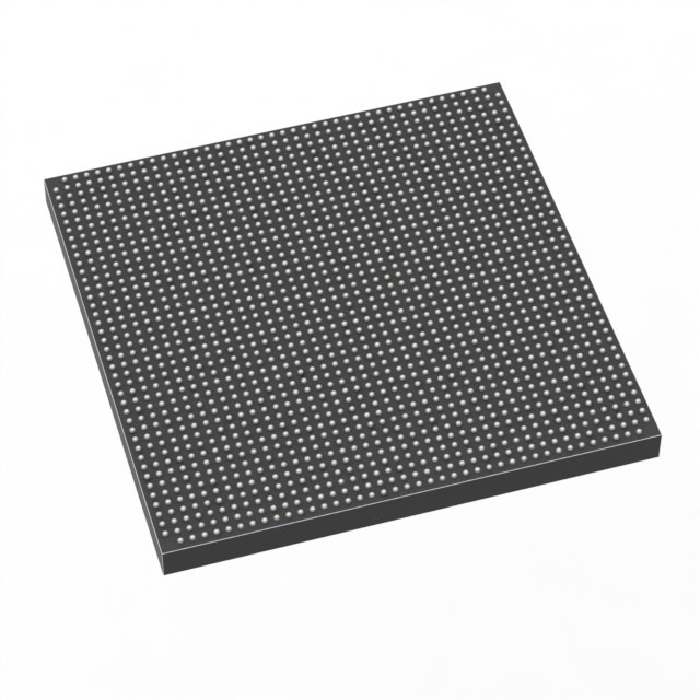
| Device Package | 1152-HBGA (42.5x42.5) | Grade | Commercial | Operating Temperature | 0°C – 85°C | ||
|---|---|---|---|---|---|---|---|
| Package / Case | 1152-BBGA, FCBGA | Number of I/O | 744 | Voltage | 870 mV - 930 mV | ||
| Mounting Method | Surface Mount | RoHS Compliance | RoHS Compliant | REACH Compliance | REACH Unaffected | ||
| Moisture Sensitivity Level | 3 (168 Hours) | Number of LABs/CLBs | 21248 | Number of Logic Elements/Cells | 531200 | ||
| Number of Gates | N/A | ECCN | N/A | HTS Code | N/A | ||
| Qualification | N/A | Total RAM Bits | 28033024 |
Overview of EP4SE530H35C2G – Field Programmable Gate Array (FPGA) IC
The EP4SE530H35C2G is a high-density FPGA device built on the Stratix IV device family architecture. It delivers a large programmable fabric with extensive on-chip memory and I/O to support high-throughput, logic‑intensive designs.
This device targets applications that require substantial logic capacity, on-chip memory, and broad I/O connectivity. Its combination of 531,200 logic elements, approximately 28 Mbits of embedded memory, and 744 I/O pins supports complex signal processing, protocol bridging, and high-bandwidth system functions.
Key Features
- Core Logic 531,200 logic elements provide a large programmable fabric for implementing complex algorithms, state machines, and custom accelerators.
- Embedded Memory Approximately 28 Mbits of on-chip RAM for buffering, frame storage, and intermediate data processing close to logic.
- I/O and Packaging 744 user I/O pins in a 1152-ball HBGA FCBGA package (42.5 × 42.5 mm) enable dense external interfacing and system routing.
- Stratix IV Architecture Device handbook documents architecture features including clock networks, PLLs, DSP blocks, and high-speed transceiver support for protocol and bandwidth flexibility.
- Power Core supply range specified from 870 mV to 930 mV to meet system power-rail requirements for the device core.
- Operating Range & Grade Commercial grade with an operating temperature range of 0 °C to 85 °C, suitable for standard commercial applications.
- Regulatory RoHS compliant for lead-free assembly and environmental compliance.
Typical Applications
- High-Speed Data Interfaces Implement protocol bridging, packet processing, or custom transceiver logic using the Stratix IV architecture and extensive I/O.
- Signal Processing & Acceleration Deploy DSP blocks and the large logic fabric for video, communications, or algorithmic acceleration where on-chip memory reduces external bandwidth needs.
- Prototyping & System Integration Use the device for development platforms and system prototypes that require high logic density and broad external connectivity.
- Test & Measurement Build custom acquisition, preprocessing, or real-time analysis functions leveraging the device’s memory and logic resources.
Unique Advantages
- Large Logic Capacity: 531,200 logic elements give designers the room to implement complex, multi-function systems on a single device.
- Substantial On-Chip Memory: Approximately 28 Mbits of embedded RAM reduce reliance on external memory for many buffering and processing tasks.
- Extensive I/O Count: 744 I/O pins in a high-density 1152-ball package simplify connectivity to DDR, SERDES PHYs, sensors, and external peripherals.
- Stratix IV Feature Set: Architecture features documented in the device handbook—such as clock networks, PLLs, DSP resources, and high-speed transceiver support—help implement timing-critical and high-bandwidth designs.
- Commercial Grade & RoHS Compliant: Designed for commercial-temperature environments and lead-free assembly processes.
- Low-Voltage Core: Core supply specified at 870 mV–930 mV supports low-voltage system designs and power budgeting.
Why Choose EP4SE530H35C2G?
The EP4SE530H35C2G positions itself as a logic- and memory-dense FPGA option within the Stratix IV device family, suitable for designs that demand high logic counts, sizable embedded memory, and broad I/O connectivity. Its documented architecture features—clocking, DSP resources, PLLs, and high-speed transceiver capability—make it appropriate for high-throughput signal processing, protocol implementation, and system integration tasks.
For teams developing complex FPGA-based systems that require scalable logic resources, generous on-chip RAM, and a high pin-count package, the EP4SE530H35C2G offers a platform that balances integration and system-level flexibility while adhering to commercial temperature and RoHS requirements.
Request a quote or submit a pricing and availability inquiry for EP4SE530H35C2G today to evaluate it for your next high-density FPGA design.


Date Founded: 1968
Headquarters: Santa Clara, California, USA
Employees: 130,000+
Revenue: $54.23 Billion
Certifications and Memberships: ISO9001:2015, ISO14001:2015, ISO17025:2017, ISO27001:2022, ISO45001:2018, ISO50001:2018


