
EP4SGX180HF35C4G
| Part Description |
Field Programmable Gate Array (FPGA) IC |
|---|---|
| Quantity | 903 Available (as of June 18, 2026) |

| Product Category | Field Programmable Gate Array (FPGA) |
|---|---|
| Manufacturer | Intel |
| Manufacturing Status | Active |
| Manufacturer Standard Lead Time | 26 Weeks |
| Datasheet |
Specifications & Environmental
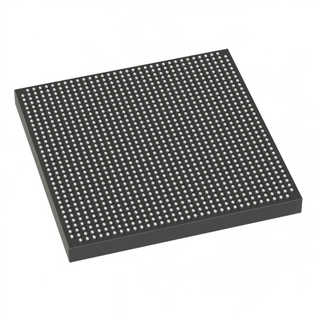
| Device Package | 1152-FBGA (35x35) | Grade | Commercial | Operating Temperature | 0°C – 85°C | ||
|---|---|---|---|---|---|---|---|
| Package / Case | 1152-BBGA, FCBGA | Number of I/O | 564 | Voltage | 870 mV - 930 mV | ||
| Mounting Method | Surface Mount | RoHS Compliance | RoHS Compliant | REACH Compliance | REACH Unaffected | ||
| Moisture Sensitivity Level | 3 (168 Hours) | Number of LABs/CLBs | 7030 | Number of Logic Elements/Cells | 175750 | ||
| Number of Gates | N/A | ECCN | N/A | HTS Code | N/A | ||
| Qualification | N/A | Total RAM Bits | 13954048 |
Overview of EP4SGX180HF35C4G – Field Programmable Gate Array (FPGA) IC
The EP4SGX180HF35C4G is a Field Programmable Gate Array from Intel’s Stratix IV device family. It delivers a high-density programmable fabric with architecture-level features documented in the Stratix IV Device Handbook.
With approximately 175,750 logic elements, roughly 13.95 Mbits of embedded memory, 564 I/O pins and integrated high‑speed transceiver features, this commercial‑grade, surface‑mount FCBGA device targets high‑performance designs that require large logic capacity, substantial on‑chip memory and extensive I/O integration.
Key Features
- Logic Capacity Approximately 175,750 logic elements for implementing large, complex digital systems and custom accelerators.
- Embedded Memory Total on‑chip RAM of 13,954,048 bits (approximately 13.95 Mbits) to support buffers, FIFOs and local data storage.
- I/O and Packaging 564 I/O pins in a 1152‑FBGA (35×35) FCBGA package, surface mount, enabling dense board‑level integration.
- Supply and Thermal Typical voltage supply range of 870 mV to 930 mV and an operating temperature range of 0 °C to 85 °C (commercial grade).
- High‑Speed Transceiver and I/O Features Device family documentation highlights high‑speed differential I/O, DPA and Soft‑CDR capabilities and broad protocol support suitable for serial link applications.
- Architecture and System Features Stratix IV family architecture includes embedded memory, DSP blocks, clock networks and PLLs, as described in the device handbook, to support timing, signal integrity and system integration.
- Compliance RoHS compliant, meeting standard lead‑free environmental requirements.
Typical Applications
- High‑performance Networking & Telecom Leverage the device’s high logic density, large embedded memory and documented high‑speed transceiver features for packet processing, switching and protocol adaptation.
- Digital Signal Processing Use the substantial logic resources and on‑chip RAM to implement DSP pipelines, filtering, and real‑time data processing engines.
- Memory Interface and Buffering Combine the device’s embedded memory and I/O capability for memory controller logic, buffering and external memory interface designs.
- Custom Accelerators Deploy the programmable fabric to create application‑specific accelerators that require significant parallel logic and local storage.
Unique Advantages
- High logic density: Approximately 175,750 logic elements enable large-scale designs without immediate partitioning across multiple devices.
- Substantial on‑chip memory: Approximately 13.95 Mbits of embedded RAM reduces dependence on external memory for many buffering and caching needs.
- Extensive I/O: 564 I/O pins in a compact 1152‑FBGA package allow flexible interfacing to peripherals and high‑pin‑count subsystems.
- Stratix IV architecture: Family features such as DSP blocks, PLLs and clock networks provide architecture-level building blocks for timing, synchronization and signal processing.
- High‑speed serial capability: Documented high‑speed transceiver and differential I/O features support serial link and protocol implementations referenced in the device handbook.
- Commercial‑grade and RoHS‑compliant: Designed for commercial temperature ranges (0 °C to 85 °C) and compliant with RoHS requirements for lead‑free manufacture.
Why Choose EP4SGX180HF35C4G?
The EP4SGX180HF35C4G positions itself as a high‑capacity Stratix IV FPGA for designs requiring significant logic resources, on‑chip memory and a large I/O complement. Its documented architecture and transceiver features make it suitable for demanding communication, signal processing and custom acceleration tasks.
Engineers and system designers who need scalable programmable logic with integrated memory, DSP capabilities and robust I/O options will find this device suitable for complex, high‑integration applications. Backed by the Stratix IV device documentation, it provides a well‑characterized platform for long‑lifecycle designs and system integration.
Request a quote or submit a purchasing inquiry to receive pricing, availability and lead‑time information for the EP4SGX180HF35C4G.


Date Founded: 1968
Headquarters: Santa Clara, California, USA
Employees: 130,000+
Revenue: $54.23 Billion
Certifications and Memberships: ISO9001:2015, ISO14001:2015, ISO17025:2017, ISO27001:2022, ISO45001:2018, ISO50001:2018


