
EP4SGX180HF35C4N
| Part Description |
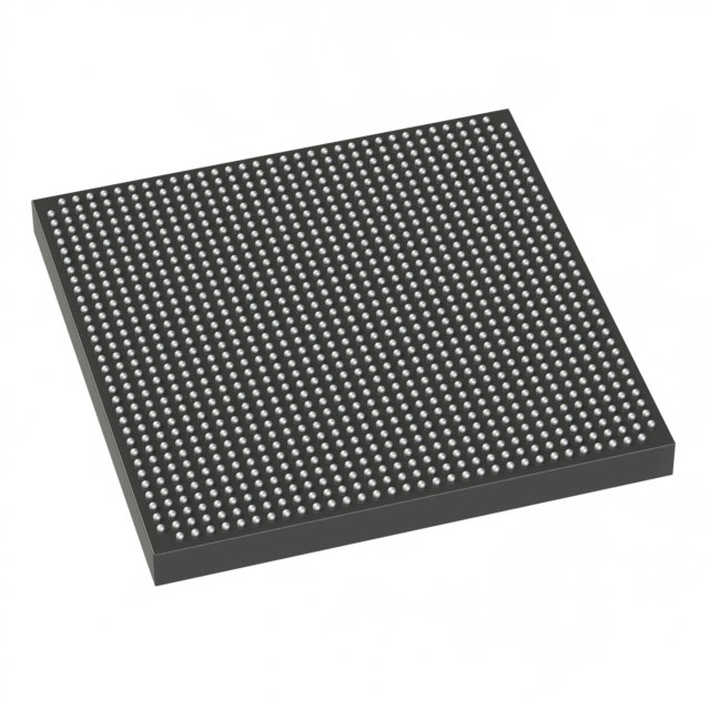
Stratix® IV GX Field Programmable Gate Array (FPGA) IC 564 13954048 175750 1152-BBGA, FCBGA |
|---|---|
| Quantity | 1,213 Available (as of June 18, 2026) |

| Product Category | Field Programmable Gate Array (FPGA) |
|---|---|
| Manufacturer | Intel |
| Manufacturing Status | Obsolete |
| Manufacturer Standard Lead Time | Contact Us |
| Datasheet |
Specifications & Environmental
| Device Package | 1152-FBGA (35x35) | Grade | Commercial | Operating Temperature | 0°C – 85°C | ||
|---|---|---|---|---|---|---|---|
| Package / Case | 1152-BBGA, FCBGA | Number of I/O | 564 | Voltage | 870 mV - 930 mV | ||
| Mounting Method | Surface Mount | RoHS Compliance | RoHS Compliant | REACH Compliance | REACH Unknown | ||
| Moisture Sensitivity Level | 3 (168 Hours) | Number of LABs/CLBs | 7030 | Number of Logic Elements/Cells | 175750 | ||
| Number of Gates | N/A | ECCN | 3A001A7A | HTS Code | 8542.39.0001 | ||
| Qualification | N/A | Total RAM Bits | 13954048 |
Overview of EP4SGX180HF35C4N – Stratix® IV GX Field Programmable Gate Array (FPGA) IC
The EP4SGX180HF35C4N is an Intel Stratix IV GX FPGA family device offering high logic density and extensive I/O in a 1152‑ball FCBGA package. It targets designs that require large on‑chip memory, significant logic resources, and high‑speed I/O capability.
With 175,750 logic elements and approximately 13.95 Mbits of embedded memory, this commercial‑grade FPGA is suited for systems that demand high aggregate data bandwidth, flexible FPGA fabric and I/O features, and integrated DSP and clocking resources as described in the device handbook.
Key Features
- High Logic Density — 175,750 logic elements to implement complex digital functions, state machines, and custom hardware acceleration.
- Embedded Memory — Approximately 13.95 Mbits of on‑chip RAM for buffering, packet processing, and local storage of intermediate data.
- Extensive I/O — 564 I/O pins to support wide external connectivity and multiple parallel interfaces.
- High‑Speed Transceiver and I/O Architecture — Device handbook lists high‑speed differential I/O and transceiver features designed to support high aggregate data bandwidth and a wide range of protocol support.
- DSP and Clocking Resources — Includes dedicated digital signal processing blocks and PLL/clock network features referenced in the Stratix IV device handbook for timing and signal processing tasks.
- Power and Supply — Specified core voltage supply range of 870 mV to 930 mV to match system power design requirements.
- Package and Mounting — 1152‑BBGA FCBGA package (supplier package: 1152‑FBGA, 35×35) with surface‑mount construction for board‑level integration.
- Commercial Temperature Grade — Rated for 0 °C to 85 °C ambient operation, suitable for commercial applications.
- RoHS Compliant — Conforms to RoHS environmental requirements for lead‑free manufacturing.
Typical Applications
- High‑bandwidth Networking and Communications — Use where high aggregate data throughput and high‑speed I/O/transceiver support are required.
- Memory Interface and Controller Design — Leverage abundant I/O and embedded memory for external memory interfaces and buffering tasks.
- DSP‑intensive Systems — Implement signal processing chains and hardware accelerators using the device’s DSP resources and large logic fabric.
- System Integration and Prototyping — Consolidate multiple functions into a single FPGA for complex system prototypes and integration tasks.
Unique Advantages
- Substantial Logic Capacity: 175,750 logic elements allow implementation of large custom circuits and multiple subsystems in one device, reducing board-level component count.
- Significant On‑Chip RAM: Approximately 13.95 Mbits of embedded memory supports deep buffering and local data storage without relying solely on external memory.
- Broad I/O Count: 564 I/O pins provide flexibility for parallel interfaces, multiple peripheral connections, and wide data buses.
- Commercial‑grade Readiness: 0 °C to 85 °C operating range and RoHS compliance align with standard commercial product and assembly requirements.
- Integrated Clocking and DSP Resources: On‑chip PLLs, clock networks, and DSP blocks referenced in the device handbook simplify timing and signal processing implementation.
- Industry‑recognized FPGA Family: Stratix IV GX architecture features documented high‑speed transceiver and protocol support, aiding design planning for high‑throughput applications.
Why Choose EP4SGX180HF35C4N?
The EP4SGX180HF35C4N positions itself for designs that require a combination of high logic density, substantial embedded memory, and wide I/O capability in a commercial‑grade FPGA. Its feature set—called out in the Stratix IV device handbook—supports developers implementing high‑bandwidth interfaces, DSP workloads, and complex system integration on a single programmable device.
This part is well suited for engineers and teams building scalable hardware where on‑chip resources, configurable fabric, and documented transceiver/I/O architectures are key to meeting system throughput and integration goals.
Request a quote or submit an inquiry to obtain pricing, availability, and technical support for the EP4SGX180HF35C4N.


Date Founded: 1968
Headquarters: Santa Clara, California, USA
Employees: 130,000+
Revenue: $54.23 Billion
Certifications and Memberships: ISO9001:2015, ISO14001:2015, ISO17025:2017, ISO27001:2022, ISO45001:2018, ISO50001:2018


