
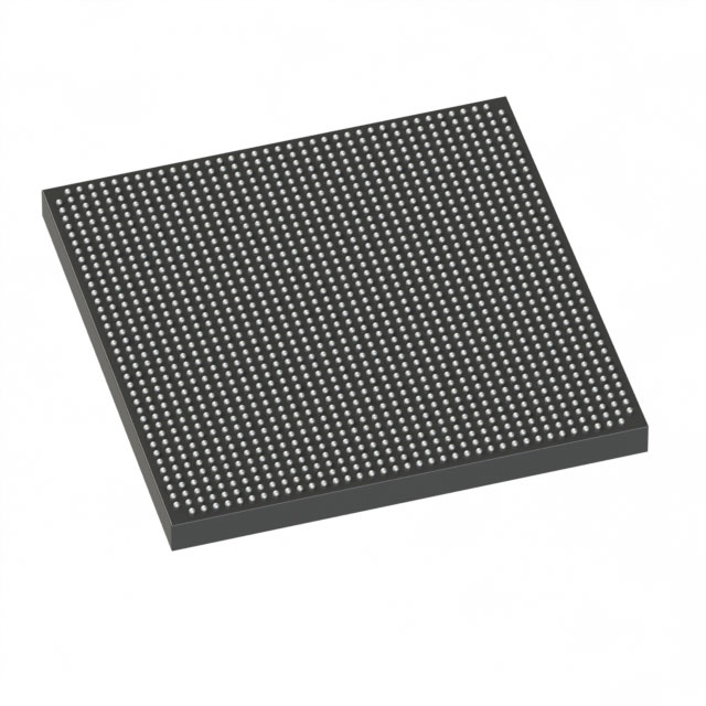
EP4SGX180KF40C2
| Part Description |
Stratix® IV GX Field Programmable Gate Array (FPGA) IC 744 13954048 175750 1517-BBGA, FCBGA |
|---|---|
| Quantity | 1,011 Available (as of June 15, 2026) |
| Product Category | Field Programmable Gate Array (FPGA) |
|---|---|
| Manufacturer | Intel |
| Manufacturing Status | Obsolete |
| Manufacturer Standard Lead Time | Contact Us |
| Datasheet |
Specifications & Environmental
| Device Package | 1517-FBGA (40x40) | Grade | Commercial | Operating Temperature | 0°C – 85°C | ||
|---|---|---|---|---|---|---|---|
| Package / Case | 1517-BBGA, FCBGA | Number of I/O | 744 | Voltage | 870 mV - 930 mV | ||
| Mounting Method | Surface Mount | RoHS Compliance | RoHS non-compliant | REACH Compliance | REACH Unknown | ||
| Moisture Sensitivity Level | 3 (168 Hours) | Number of LABs/CLBs | 7030 | Number of Logic Elements/Cells | 175750 | ||
| Number of Gates | N/A | ECCN | 3A001A7A | HTS Code | 8542.39.0001 | ||
| Qualification | N/A | Total RAM Bits | 13954048 |
Overview of EP4SGX180KF40C2 – Stratix IV GX FPGA, 175,750 logic elements, 744 I/O
The EP4SGX180KF40C2 is a Stratix® IV GX Field Programmable Gate Array (FPGA) in a 1517-BBGA FCBGA package. It combines high logic density with on-chip embedded memory and an extensive I/O complement for complex system integration tasks.
As part of the Stratix IV family, this device targets high-bandwidth designs that benefit from high aggregate data throughput, high-speed transceiver features, DSP capability and flexible external memory interfacing as described in the Stratix IV Device Handbook.
Key Features
- Core Logic — 175,750 logic elements provide substantial programmable capacity for complex digital designs.
- Logic Array Blocks — Built from a fabric architecture consistent with Stratix IV GX devices and documented in the Stratix IV Device Handbook, supporting sophisticated logic partitioning and timing strategies.
- Embedded Memory — Approximately 13.95 Mbits of on-chip RAM to support buffering, frame storage, and scratch memory without external devices.
- I/O Capacity — 744 I/O pins to accommodate wide buses, multiple peripheral interfaces and dense external connectivity.
- High-Speed Interfaces — Device handbook notes high-speed transceiver features, wide protocol support and external memory interface capabilities suitable for high-throughput designs.
- Clocking and DSP — Includes dedicated clock networks, PLLs and documented DSP block support in the Stratix IV family for deterministic timing and signal processing tasks.
- Power — Core voltage range specified at 870 mV to 930 mV for defined power-rail planning.
- Package & Mounting — Package case: 1517-BBGA, FCBGA; supplier device package: 1517-FBGA (40×40). Surface-mount mounting type for standard board assembly processes.
- Operating Range & Grade — Commercial grade operation from 0 °C to 85 °C.
- Compliance — RoHS compliant.
Typical Applications
- High-Bandwidth Communications — Leverage the Stratix IV GX high-speed transceiver features and wide protocol support for line cards, transport and backplane interfacing.
- Networking and Packet Processing — High logic density and abundant I/O enable complex packet handling, traffic management and protocol acceleration functions.
- Video and Imaging Systems — Large on-chip RAM and DSP resources support frame buffering, preprocessing and real-time pipeline operations.
- High-Speed Interface Bridging — Use the device’s extensive I/O and external memory interface capabilities to bridge between multiple high-speed peripherals and memory subsystems.
Unique Advantages
- High Logic Capacity: 175,750 logic elements let you integrate large functions and multiple subsystems on a single device, reducing board-level complexity.
- Significant On‑Chip Memory: Approximately 13.95 Mbits of embedded memory reduces the need for external RAM for many buffering and storage tasks.
- Extensive I/O Count: 744 I/O pins support wide parallel buses and numerous interfaces without multiplexing compromises.
- Designed for High Throughput: Stratix IV GX family features in the device handbook highlight high-speed transceivers and broad protocol support for demanding data-rate applications.
- Defined Power Envelope: Core voltage specified between 870 mV and 930 mV aids in accurate power budgeting during design.
- Commercial Temperature and RoHS: Rated for 0 °C to 85 °C operation and RoHS compliant for general-purpose commercial deployments.
Why Choose EP4SGX180KF40C2?
The EP4SGX180KF40C2 brings Stratix IV GX family architecture to designs that require large programmable resources, extensive I/O and substantial on-chip memory. Its documented high-speed transceiver and system integration features make it suitable for throughput‑oriented applications where on-device logic and memory reduce external component count.
This device is well suited to engineering teams building complex communications, networking, imaging or high-speed interface products who need a commercially rated FPGA with high logic density, abundant I/O and documented Stratix IV family capabilities.
Request a quote or submit an inquiry to obtain pricing and availability for the EP4SGX180KF40C2. Our team can provide further ordering and technical information to support your design evaluation.


Date Founded: 1968
Headquarters: Santa Clara, California, USA
Employees: 130,000+
Revenue: $54.23 Billion
Certifications and Memberships: ISO9001:2015, ISO14001:2015, ISO17025:2017, ISO27001:2022, ISO45001:2018, ISO50001:2018


