
EP4SGX230HF35C2
| Part Description |
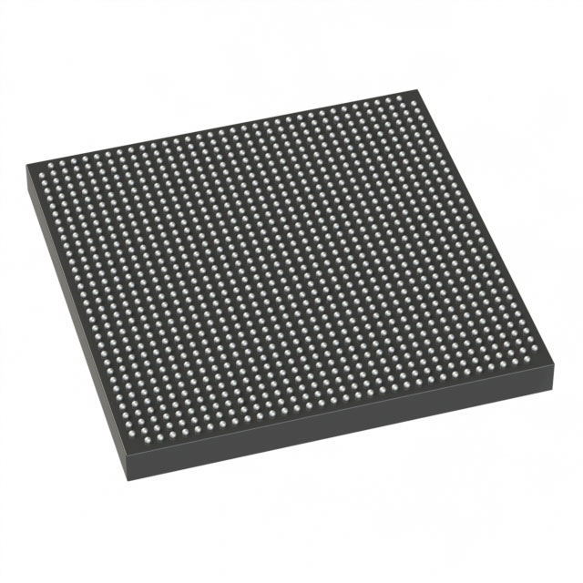
Stratix® IV GX Field Programmable Gate Array (FPGA) IC 564 17544192 228000 1152-BBGA, FCBGA |
|---|---|
| Quantity | 1,556 Available (as of June 10, 2026) |

| Product Category | Field Programmable Gate Array (FPGA) |
|---|---|
| Manufacturer | Intel |
| Manufacturing Status | Obsolete |
| Manufacturer Standard Lead Time | Contact Us |
| Datasheet |
Specifications & Environmental
| Device Package | 1152-FBGA (35x35) | Grade | Commercial | Operating Temperature | 0°C – 85°C | ||
|---|---|---|---|---|---|---|---|
| Package / Case | 1152-BBGA, FCBGA | Number of I/O | 564 | Voltage | 870 mV - 930 mV | ||
| Mounting Method | Surface Mount | RoHS Compliance | RoHS non-compliant | REACH Compliance | REACH Unknown | ||
| Moisture Sensitivity Level | 3 (168 Hours) | Number of LABs/CLBs | 9120 | Number of Logic Elements/Cells | 228000 | ||
| Number of Gates | N/A | ECCN | 3A001A7A | HTS Code | 8542.39.0001 | ||
| Qualification | N/A | Total RAM Bits | 17544192 |
Overview of EP4SGX230HF35C2 – Stratix® IV GX Field Programmable Gate Array (FPGA) IC, 228000 logic elements, 1152-BBGA
The EP4SGX230HF35C2 is an Intel Stratix IV GX Field Programmable Gate Array (FPGA) provided in a 1152-BBGA (35×35) surface-mount package. The device offers a high logic density architecture accompanied by on-chip memory and extensive I/O, and is documented in the Stratix IV Device Handbook device datasheet.
Design documentation for this device includes sections covering transceiver performance, DSP block specifications, TriMatrix memory blocks, PLLs and clock-tree specification, and configuration/JTAG behavior—making the device suitable for designs that require integrated transceivers, signal processing resources, and flexible clocking and configuration options.
Key Features
- Core Logic 228,000 logic elements provide high integration density for complex FPGA implementations.
- Embedded Memory Approximately 17.5 Mbits of on-chip RAM (Total Ram Bits: 17,544,192) for data buffering, lookup tables and state storage.
- I/O Resources 564 user I/Os to support broad peripheral connectivity and multiple high-pin-count interfaces.
- Transceivers & DSP Blocks Device documentation includes transceiver performance specifications and DSP block specifications for implementation of serial links and DSP-accelerated functions.
- Clocking and Configuration Stratix IV device handbook content covers PLL specifications, clock-tree details, and configuration/JTAG support for system timing and bring-up.
- Power Core supply range specified at 0.870 V to 0.930 V to match system power-rail planning for the FPGA core.
- Package & Mounting 1152-FBGA (35×35) FCBGA package, surface-mount, intended for compact board-level integration.
- Temperature & Grade Commercial grade with an operating temperature range of 0 °C to 85 °C.
- Compliance RoHS compliant.
Typical Applications
- High-speed communications Leverages the device’s transceiver performance documentation and high I/O count for implementing serial links and protocol bridging.
- DSP and signal processing DSP block specifications and substantial on-chip memory support algorithm acceleration and streaming data processing.
- Data acquisition and buffering Large embedded memory and plentiful I/O make the device suitable for front-end data capture, buffering, and preprocessing tasks.
- System integration and prototyping High logic density and configurable clocking/PLL options assist in consolidating multiple system functions into a single FPGA device.
Unique Advantages
- High logic density: 228,000 logic elements enable complex designs and feature consolidation on a single device.
- Substantial on-chip memory: Approximately 17.5 Mbits of embedded RAM reduces external memory dependency for many buffering and stateful functions.
- Extensive I/O availability: 564 user I/Os support a wide range of peripherals and parallel interfaces without extra IO expansion components.
- Integrated transceiver and DSP documentation: Dedicated datasheet sections for transceivers and DSP blocks simplify evaluation and implementation of high-throughput and signal-processing features.
- Compact FCBGA package: 1152-FBGA (35×35) package supports dense PCB layouts and surface-mount assembly.
- Clear operating envelope: Commercial grade operation from 0 °C to 85 °C with specified core supply range (0.870–0.930 V) for predictable system integration.
Why Choose EP4SGX230HF35C2?
The EP4SGX230HF35C2 positions itself for designs that demand high logic capacity, significant on-chip memory, and extensive I/O in a compact FCBGA package. With detailed documentation covering transceiver performance, DSP block behavior, clocking/PLL, and configuration, the device supports complex FPGA implementations where integrated serial interfaces and signal-processing resources are required.
This Stratix IV GX device is appropriate for engineering teams consolidating multi-function systems or building throughput- and memory-heavy designs that benefit from tight integration and a defined operating specification. Device-level documentation in the Stratix IV Device Handbook provides the technical detail needed for migration from prototype to production designs.
Request a quote or submit a pricing request to discuss availability, lead times, and quantity pricing for EP4SGX230HF35C2.


Date Founded: 1968
Headquarters: Santa Clara, California, USA
Employees: 130,000+
Revenue: $54.23 Billion
Certifications and Memberships: ISO9001:2015, ISO14001:2015, ISO17025:2017, ISO27001:2022, ISO45001:2018, ISO50001:2018


