
EP4SGX360KF43C3G
| Part Description |
Field Programmable Gate Array (FPGA) IC |
|---|---|
| Quantity | 1,019 Available (as of June 18, 2026) |

| Product Category | Field Programmable Gate Array (FPGA) |
|---|---|
| Manufacturer | Intel |
| Manufacturing Status | Active |
| Manufacturer Standard Lead Time | 26 Weeks |
| Datasheet |
Specifications & Environmental
| Device Package | 1760-FCBGA (42.5x42.5) | Grade | Commercial | Operating Temperature | 0°C – 85°C | ||
|---|---|---|---|---|---|---|---|
| Package / Case | 1760-BBGA, FCBGA | Number of I/O | 880 | Voltage | 870 mV - 930 mV | ||
| Mounting Method | Surface Mount | RoHS Compliance | RoHS Compliant | REACH Compliance | REACH Unaffected | ||
| Moisture Sensitivity Level | 3 (168 Hours) | Number of LABs/CLBs | 14144 | Number of Logic Elements/Cells | 353600 | ||
| Number of Gates | N/A | ECCN | N/A | HTS Code | N/A | ||
| Qualification | N/A | Total RAM Bits | 23105536 |
Overview of EP4SGX360KF43C3G – Field Programmable Gate Array (FPGA) IC
The EP4SGX360KF43C3G is a commercial‑grade Stratix IV family FPGA from Intel, delivered in a high‑density FCBGA package. It combines a large logic fabric with substantial embedded memory and extensive I/O resources to address demanding digital design tasks.
With 353,600 logic elements and approximately 23 Mbits of embedded memory, this device targets applications that require high aggregate data bandwidth, complex signal processing, and broad external interfacing while operating from a low core supply voltage.
Key Features
- Core Logic: 353,600 logic elements provide a substantial programmable fabric for implementing complex digital functions and custom accelerators.
- Embedded Memory: Approximately 23 Mbits of on‑chip RAM to support buffering, packet storage, and on‑FPGA data structures.
- I/O Capacity: Up to 880 user I/O pins enable wide external connectivity and parallel interfaces for memory, sensors, and peripherals.
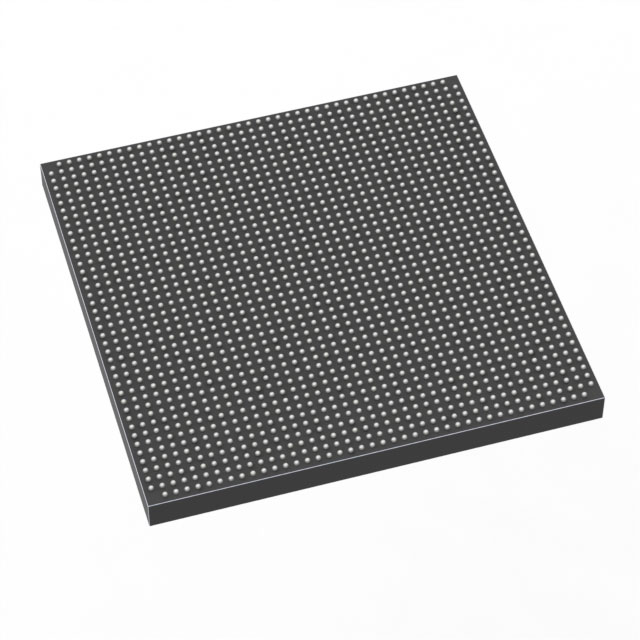
- Package & Mounting: 1760‑pin FCBGA (1760‑FCBGA, 42.5 × 42.5 mm) in a surface‑mount format for high‑density board integration.
- Power Supply: Core voltage supply range of 870 mV to 930 mV, consistent with low‑voltage FPGA core operation.
- Operating Temperature & Grade: Commercial grade with an operating temperature range of 0 °C to 85 °C.
- Architecture Features (series handbook): Device documentation highlights Stratix IV architecture features including embedded DSP blocks, PLLs, clock networks, and high‑speed transceiver capability for high‑bandwidth designs.
- Compliance: RoHS compliant, meeting common environmental requirements for electronic assemblies.
Typical Applications
- High‑bandwidth communications: Large logic capacity and references to high‑speed transceiver features make the device suitable for packet processing, interface bridging, and protocol handling.
- Signal processing and acceleration: Substantial logic and embedded memory, together with documented DSP block support in the device family, enable on‑chip data path acceleration and real‑time processing.
- Memory interface and buffering: The combination of many I/O pins and significant on‑chip RAM supports external memory interfacing, buffering, and complex memory controllers.
- Custom compute and system integration: High logic density and extensive I/O allow integration of multiple system functions—control, data plane, and interface logic—into a single FPGA package.
Unique Advantages
- High logic capacity: 353,600 logic elements enable implementation of large, partitioned designs or densely packed custom logic blocks.
- Substantial on‑chip memory: Approximately 23 Mbits of embedded RAM reduces reliance on external memory for intermediate storage and accelerates data‑intensive operations.
- Extensive I/O resources: 880 I/O pins offer flexibility for parallel interfaces, wide buses, and multiple peripheral connections without external multiplexing.
- Dense, board‑level integration: 1760‑pin FCBGA package (42.5 × 42.5 mm) supports compact, high‑density PCB layouts for space‑constrained systems.
- Low core voltage operation: Narrow supply window (870–930 mV) reflects optimized core power delivery for the device family’s fabrication and architecture.
- Documented architecture: The Stratix IV device handbook provides architecture-level detail—clocking, PLLs, DSP resources, and transceiver features—helpful for system design and validation.
Why Choose EP4SGX360KF43C3G?
EP4SGX360KF43C3G positions itself as a high‑capacity, commercial‑grade FPGA for designs that demand significant programmable logic, on‑chip memory, and broad I/O. Its combination of 353,600 logic elements, roughly 23 Mbits of embedded RAM, and 880 I/O pins supports integrated system designs where consolidation of functions and flexible interfacing are priorities.
Backed by Intel’s Stratix IV family documentation, the device is suitable for development teams needing an FPGA platform with documented architecture features such as DSP blocks, PLLs, clock networks, and high‑speed transceiver capability. This makes it a practical choice for teams building high‑bandwidth, compute‑intensive, or multi‑interface applications within commercial operating conditions.
Request a quote or submit an inquiry to evaluate EP4SGX360KF43C3G for your next design, and to obtain pricing and availability information.


Date Founded: 1968
Headquarters: Santa Clara, California, USA
Employees: 130,000+
Revenue: $54.23 Billion
Certifications and Memberships: ISO9001:2015, ISO14001:2015, ISO17025:2017, ISO27001:2022, ISO45001:2018, ISO50001:2018


