
EPF10K100ARC240-2
| Part Description |
FLEX-10KA® Field Programmable Gate Array (FPGA) IC 189 24576 4992 240-BFQFP Exposed Pad |
|---|---|
| Quantity | 1,474 Available (as of June 15, 2026) |

| Product Category | Field Programmable Gate Array (FPGA) |
|---|---|
| Manufacturer | Intel |
| Manufacturing Status | Obsolete |
| Manufacturer Standard Lead Time | Contact Us |
| Datasheet |
Specifications & Environmental
| Device Package | 240-RQFP (32x32) | Grade | Commercial | Operating Temperature | 0°C – 70°C | ||
|---|---|---|---|---|---|---|---|
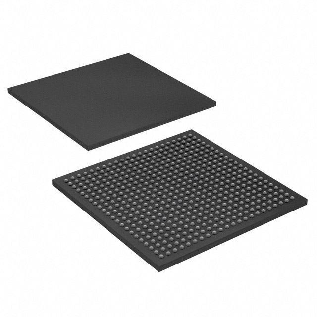
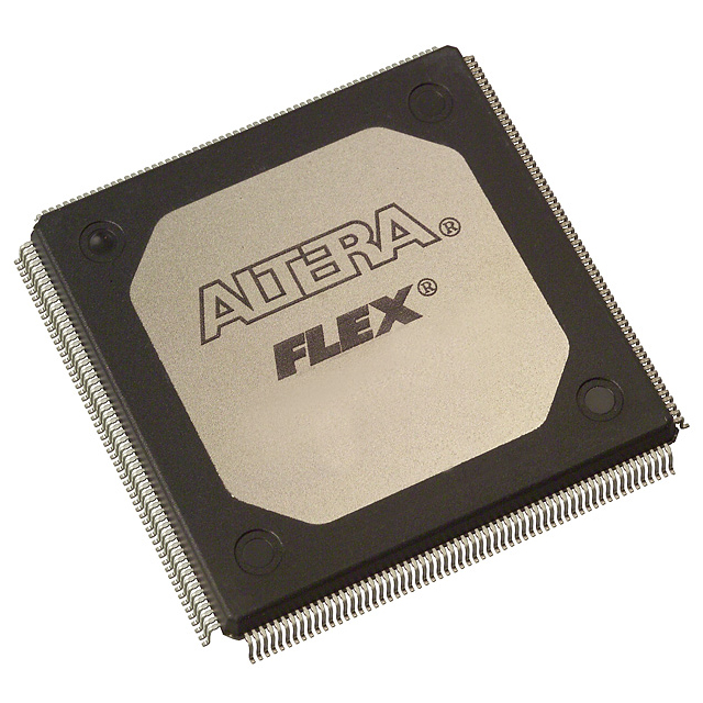
| Package / Case | 240-BFQFP Exposed Pad | Number of I/O | 189 | Voltage | 3 V - 3.6 V | ||
| Mounting Method | Surface Mount | RoHS Compliance | RoHS non-compliant | REACH Compliance | REACH Unaffected | ||
| Moisture Sensitivity Level | 6 (Time on Label) | Number of LABs/CLBs | 624 | Number of Logic Elements/Cells | 4992 | ||
| Number of Gates | 158000 | ECCN | 3A991D | HTS Code | 8542.39.0001 | ||
| Qualification | N/A | Total RAM Bits | 24576 |
Overview of EPF10K100ARC240-2 – FLEX-10KA FPGA, 4,992 Logic Elements, 24,576 RAM bits, 189 I/Os, 240‑BFQFP
The EPF10K100ARC240-2 is a FLEX‑10KA family field programmable gate array (FPGA) offering embedded programmable logic intended for system-level integration. It combines an embedded array for implementing megafunctions with a general-purpose logic array to deliver flexible on‑chip functionality.
With 4,992 logic elements, 24,576 bits of on‑chip RAM, and 189 user I/O pins in a 240‑BFQFP exposed‑pad package, this commercial‑grade device targets designs that require moderate logic density, substantial embedded memory, and a high pin count while operating from a 3.0 V to 3.6 V supply.
Key Features
- Core architecture Embedded programmable logic device architecture combining an embedded array for megafunctions (efficient memory and specialized logic) with a separate logic array for general logic functions.
- Logic capacity 4,992 logic elements and 158,000 gates (specified) provide medium-density programmable logic for a wide range of designs.
- Embedded memory 24,576 total RAM bits of on‑chip memory to implement buffers, FIFOs, or other memory‑centric megafunctions without consuming general logic resources.
- I/O capability 189 user I/O pins offering high pin count for parallel interfaces and board-level integration; FLEX 10KA family supports MultiVolt I/O and 5.0‑V tolerant input pins.
- Configuration and test In‑circuit reconfigurability options and built‑in JTAG boundary‑scan (IEEE 1149.1) for device programming and board‑level test without consuming user logic.
- Clock and routing features Dedicated carry and cascade chains and family options such as ClockLock and ClockBoost (series features) for predictable interconnect and clock management.
- Package and mounting Surface‑mount 240‑BFQFP exposed pad package (supplier package 240‑RQFP, 32×32) for placement on compact PCBs while providing thermal benefit via the exposed pad.
- Power and environmental Operates from a 3.0 V to 3.6 V supply and specified for commercial temperature range of 0 °C to 70 °C; RoHS compliant.
Typical Applications
- System‑on‑a‑Programmable‑Chip (SOPC) Integration — Use the embedded arrays and logic fabric to consolidate memory, interface logic, and custom functions into a single programmable device for tighter system integration.
- Memory‑centric Functions — On‑chip RAM is suitable for implementing buffers, FIFOs, and other megafunctions that reduce external memory requirements and simplify board design.
- PCI and Peripheral Interfaces — FLEX 10K/10KA family support for PCI and dedicated I/O flexibility make this device appropriate for bridging, protocol handling, and high‑pin peripheral interfacing.
- Prototyping and Feature Integration — Medium‑density logic and substantial I/O count support rapid iteration and consolidation of multiple discrete functions during development and early production.
Unique Advantages
- Balanced logic and memory in one device: 4,992 logic elements combined with 24,576 bits of embedded RAM reduce the need for external logic and memory ICs.
- High I/O count for flexible system integration: 189 user I/Os enable parallel interfaces and board‑level consolidation without multiplexing compromises.
- Family features for predictable timing: Dedicated carry/cascade chains and clock options (ClockLock/ClockBoost) support efficient arithmetic and low‑skew clocking in design flows.
- Built‑in programming and testability: In‑circuit reconfigurability and IEEE 1149.1 JTAG boundary‑scan simplify programming, validation, and board test.
- Compact, manufacturable package: 240‑BFQFP exposed pad surface mount package provides a balance of pin count and board footprint with improved thermal contact via the exposed pad.
- Commercial readiness and compliance: Commercial temperature grading (0 °C to 70 °C) and RoHS compliance suit mainstream electronics production and regulatory requirements.
Why Choose EPF10K100ARC240-2?
The EPF10K100ARC240-2 positions itself as a practical, medium‑density FLEX‑10KA FPGA for designs that require significant embedded memory, a large number of I/Os, and in‑system configurability. Its combination of 4,992 logic elements, 24,576 bits of RAM, and 189 user I/O pins makes it well suited for consolidating interface logic, implementing megafunctions, and accelerating prototyping efforts.
Backed by FLEX 10K family features and development tool support cited in the series documentation, this device offers a straightforward path for engineers looking to integrate memory, custom logic, and peripheral interfaces in a single programmable component while maintaining common commercial manufacturing requirements.
Request a quote or submit an inquiry to obtain pricing, availability, and ordering information for EPF10K100ARC240-2.


Date Founded: 1968
Headquarters: Santa Clara, California, USA
Employees: 130,000+
Revenue: $54.23 Billion
Certifications and Memberships: ISO9001:2015, ISO14001:2015, ISO17025:2017, ISO27001:2022, ISO45001:2018, ISO50001:2018


