
EPF10K100AFC484-2N
| Part Description |
FLEX-10KA® Field Programmable Gate Array (FPGA) IC 369 24576 4992 484-BBGA |
|---|---|
| Quantity | 70 Available (as of June 15, 2026) |
| Product Category | Field Programmable Gate Array (FPGA) |
|---|---|
| Manufacturer | Intel |
| Manufacturing Status | Obsolete |
| Manufacturer Standard Lead Time | Contact Us |
| Datasheet |
Specifications & Environmental
| Device Package | 484-FBGA (23x23) | Grade | Commercial | Operating Temperature | 0°C – 70°C | ||
|---|---|---|---|---|---|---|---|
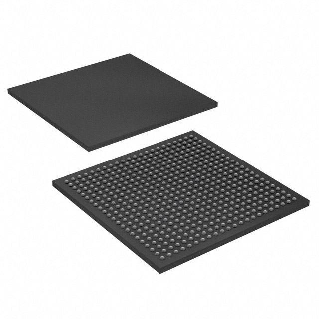
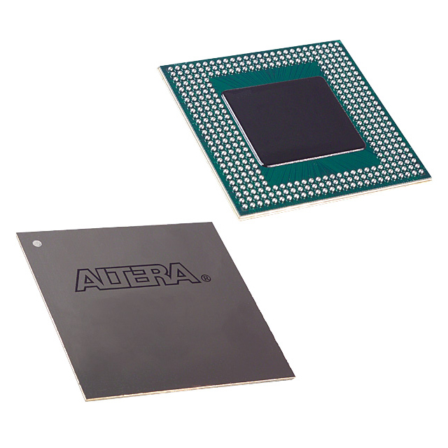
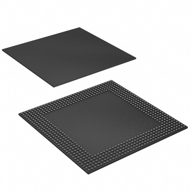
| Package / Case | 484-BBGA | Number of I/O | 369 | Voltage | 3 V - 3.6 V | ||
| Mounting Method | Surface Mount | RoHS Compliance | Unknown | REACH Compliance | REACH Unaffected | ||
| Moisture Sensitivity Level | 3 (168 Hours) | Number of LABs/CLBs | 624 | Number of Logic Elements/Cells | 4992 | ||
| Number of Gates | 158000 | ECCN | 3A001A2A | HTS Code | 8542.39.0001 | ||
| Qualification | N/A | Total RAM Bits | 24576 |
Overview of EPF10K100AFC484-2N – FLEX-10KA® FPGA, 484-BBGA
The EPF10K100AFC484-2N is a FLEX-10KA family field programmable gate array (FPGA) supplied in a 484-ball fine-pitch BGA package. It delivers a balanced combination of logic capacity, embedded RAM, and a high I/O count for system-level integration and custom logic implementation.
Designed for commercial applications, this device is suited to designs that require on-chip memory and flexible interfacing, providing 4,992 logic elements, 24,576 bits of embedded RAM, and 369 user I/O pins while operating from a 3.0 V to 3.6 V supply over a 0 °C to 70 °C temperature range.
Key Features
- Logic Capacity Approximately 4,992 logic elements enabling medium-density programmable logic and combinational/sequential designs.
- Embedded Memory 24,576 total RAM bits of on-chip memory for implementing FIFOs, buffers, and other memory-intensive megafunctions.
- I/O and Interface Flexibility 369 user I/O pins support complex external interfacing and dense board-level connectivity.
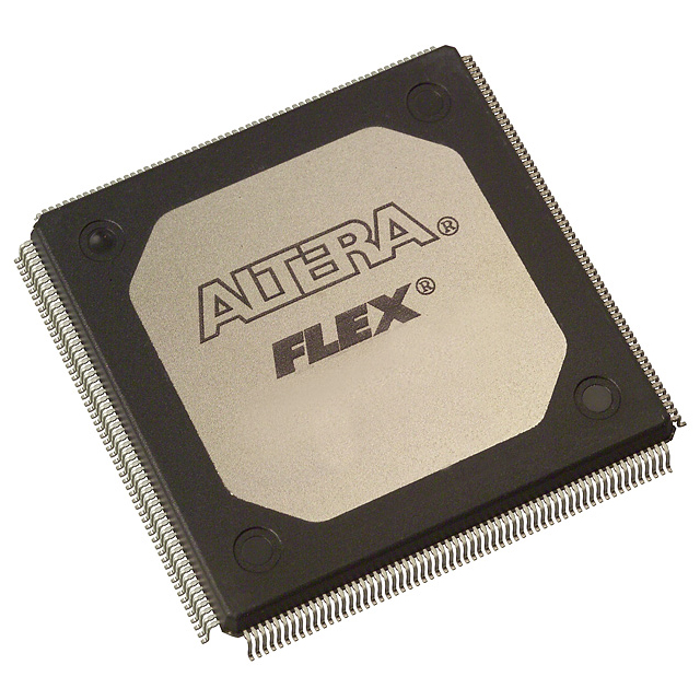
- Package and Mounting 484-ball BGA (484-FBGA, 23×23) surface-mount package for compact board integration and improved signal routing.
- Power and Temperature 3.0 V to 3.6 V supply range with commercial-grade operating temperature from 0 °C to 70 °C.
- System-Level Features Family-level capabilities include embedded arrays for megafunctions, in-circuit reconfigurability, JTAG boundary-scan support, and options such as ClockLock and ClockBoost for clock management (as provided by the FLEX 10K family).
- Manufacturing and Compliance RoHS-compliant construction to meet standard environmental requirements.
Typical Applications
- System Integration / SOPC Implement system-on-a-programmable-chip designs that combine custom logic and embedded memory for compact system architectures.
- High‑I/O Interface Bridging Use the device’s 369 I/O pins to bridge peripherals, protocol converters, or custom board-level interfaces.
- Memory and Buffering Functions Leverage the on-chip RAM to implement FIFOs, small data buffers, and scratchpad memory for dataflow control.
- Prototyping and Development Medium-density logic and flexible reconfiguration make this device suitable for hardware prototyping and iterative design cycles.
- PCI and Peripheral Subsystems Family-level support for PCI-related features enables integration into PCI-local-bus-capable designs where applicable.
Unique Advantages
- Balanced logic and memory: 4,992 logic elements combined with 24,576 bits of embedded RAM deliver a useful mix of compute and storage for mid-range designs.
- High pin-count connectivity: 369 user I/O pins enable complex external interfacing without additional bridge devices, reducing BOM and board complexity.
- Compact BGA packaging: 484-ball FBGA (23×23) minimizes board footprint while supporting dense routing for high-functionality boards.
- Family-level system features: Support for embedded arrays, JTAG boundary-scan, in-circuit reconfiguration, and clock management options simplifies system integration and debug.
- Commercial-grade suitability: Designed for 0 °C to 70 °C operation and RoHS-compliant manufacturing to meet standard commercial product requirements.
Why Choose EPF10K100AFC484-2N?
The EPF10K100AFC484-2N offers a practical balance of logic resources, embedded memory, and I/O capacity for commercial system designs that require on-chip buffering, protocol interfacing, and reconfigurable logic. Its FLEX-10KA family features provide system-level capabilities—including embedded arrays and JTAG support—useful for integrating megafunctions and simplifying board-level architecture.
This device is well suited for engineering teams building medium-density programmable solutions where compact packaging, flexible I/O, and on-chip memory improve integration, shorten development cycles, and reduce component count.
Request a quote or submit a quotation for EPF10K100AFC484-2N to check availability and pricing for your project needs.


Date Founded: 1968
Headquarters: Santa Clara, California, USA
Employees: 130,000+
Revenue: $54.23 Billion
Certifications and Memberships: ISO9001:2015, ISO14001:2015, ISO17025:2017, ISO27001:2022, ISO45001:2018, ISO50001:2018


